You are using an out of date browser. It may not display this or other websites correctly.
You should upgrade or use an alternative browser.
You should upgrade or use an alternative browser.
Chinese semiconductor industry
- Thread starter Hendrik_2000
- Start date
- Status
- Not open for further replies.
Interesting, if they are still in production that could mean they are localizing their supply chains and de-Americanizing them faster than expected.
Back when they were negotiating international treaties on trade there were supposed to be WTO regulations preventing this sort of thing from happening. Corporations were supposed to be able to sue foreign states for non compliance with contracts. Several countries balked at this though, including the US, so there is no way to enforce contracts when nation states blatantly break established business ties like this.
YMTC just recently bought semiconductor manufacturing tools from these Western companies with the expectation of using them in their factory and having maintenance and support. Amortization of tools is made over many years. The fact the West retroactively imposed controls on maintenance and support of these tools has significantly reduced their value to YMTC. Possibly all the way to zero. These sanctions also likely caused YMTC significant losses due to disruptions in production or additional expenses in switching to alternative tools.
YMTC just recently bought semiconductor manufacturing tools from these Western companies with the expectation of using them in their factory and having maintenance and support. Amortization of tools is made over many years. The fact the West retroactively imposed controls on maintenance and support of these tools has significantly reduced their value to YMTC. Possibly all the way to zero. These sanctions also likely caused YMTC significant losses due to disruptions in production or additional expenses in switching to alternative tools.
etching and deposition:
At present, YMTC's 128-layer flash memory is to stack two 64-layer strings
Substitution of domestic equipment. At present, the research and development of extremely high aspect ratio etching equipment is led by China Microelectronics. Among them, the company independently developed a 60:1 high-depth ratio etching machine in 2021. This equipment uses 400KHz instead of 2MHz as the bias RF source to obtain higher ion incident energy and collimation, making deep holes and deep holes. The size of the critical dimension of the groove etching meets the specification and is currently in the production line. At present, China Micro's 60:1 high-depth ratio etching machine is entering the stage of introducing long-term 64-layer and 128-layer production lines.
In addition, according to the company's research and development projects, it is currently developing ultra-high aspect ratio etching equipment that meets the requirements of more than 128 layers. Once the 128-layer device is successfully developed, mass production of 256-layer and above flash memory chips can be realized through only one string stacking process, and 384-layer or above mass production can be realized through two string stacking processes, combined with YMTC’s special Xtacking architecture The advantage is that Micron Hynix products will be rubbed against the ground.At present, YMTC's 128-layer flash memory is to stack two 64-layer strings
Substitution of domestic equipment. At present, the research and development of extremely high aspect ratio etching equipment is led by China Microelectronics. Among them, the company independently developed a 60:1 high-depth ratio etching machine in 2021. This equipment uses 400KHz instead of 2MHz as the bias RF source to obtain higher ion incident energy and collimation, making deep holes and deep holes. The size of the critical dimension of the groove etching meets the specification and is currently in the production line. At present, China Micro's 60:1 high-depth ratio etching machine is entering the stage of introducing long-term 64-layer and 128-layer production lines.
In addition, according to North Huachuang’s performance briefing on May 31, 2023, North Huachuang did not reply that it is developing extremely high or ultra-high aspect ratio etching equipment, and its research and development is only the development of "high aspect ratio" etching equipment (high depth in the industry) Aspect ratio generally refers to 20:1-30:1).
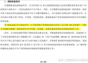

As the number of stacked layers of 3D NAND increases, the aspect ratio of the stepped contact hole will reach more than 40:1 to 60:1, which proposes higher requirements for the growth of the titanium nitride barrier layer and the filling of tungsten with extremely high aspect ratio Requirements, the increase in the number of stacked layers also requires more challenging WL line fills, including higher aspect ratios and longer lateral fills. These new processes are all realized by advanced metal CVD or ALD.
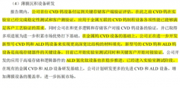
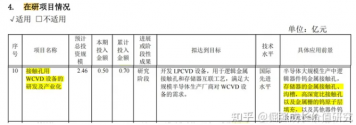
Substitution of domestic equipment. At present, the domestic "very high aspect ratio word line and contact hole tungsten filling" equipment is led by China Microelectronics. According to the 2022 annual report of Zhongwei Company, the research and development of CVD tungsten equipment and production line verification have been completed. New types of CVD tungsten and ALD tungsten equipment are being further developed to achieve material filling of structures with higher aspect ratios, and laboratory testing and verification at key clients have begun. The company said that the new CVD tungsten and ALD tungsten equipment currently under development and verification are key equipment for high-end memory devices.
Substitution of domestic equipment. At present, the domestic "very high aspect ratio word line and contact hole tungsten filling" equipment is led by China Microelectronics. According to the 2022 annual report of Zhongwei Company, the research and development of CVD tungsten equipment and production line verification have been completed. New types of CVD tungsten and ALD tungsten equipment are being further developed to achieve material filling of structures with higher aspect ratios, and laboratory testing and verification at key clients have begun. The company said that the new CVD tungsten and ALD tungsten equipment currently under development and verification are key equipment for high-end memory devices.
Cleaning: YMTC has always been reliant on ACM Research Shanghai on high tech cleaning equipment.
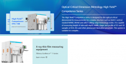
Metrology: According to research literature YMTC was reliant on KLA on yield management (inspection and so on) and thin film measurement but looks like if shifting to the nascent China metrology market, there are Chinese companies that launched or are launching metrology tools for 3D NAND between 2020-2023.
Back when they were negotiating international treaties on trade there were supposed to be WTO regulations preventing this sort of thing from happening. Corporations were supposed to be able to sue foreign states for non compliance with contracts. Several countries balked at this though, including the US, so there is no way to enforce contracts when nation states blatantly break established business ties like this.
YMTC just recently bought semiconductor manufacturing tools from these Western companies with the expectation of using them in their factory and having maintenance and support. Amortization of tools is made over many years. The fact the West retroactively imposed controls on maintenance and support of these tools has significantly reduced their value to YMTC. Possibly all the way to zero. These sanctions also likely caused YMTC significant losses due to disruptions in production or additional expenses in switching to alternative tools.
It's pretty f*cked up for US tool makers to just see 20-40 years of reputation building going down the drain due to the misunderstanding of a bunch of ignorant politicians and a bunch of humanities graduates think tankers.
Do the US is forcing a Dutch company to stop selling to what is currently one of its biggest customers - potentially the largest in the future - and is the the only one with growth in the middle of a global economic downturn? Not to mention the company is manufacturing what is effectively a niche product with few potential buyers and limited market size? Not to mention the said company already had billions sunk into developing machines meant specifically for that customer in order to comply with previous bans? Well, US better offer one hell of a compensation or I would expect the company's technology to mysteriously end up in said customer's hands. Simple market forces at work.Exclusive: US, Dutch set to hit China's chipmakers with one-two punch
June 29 (Reuters) - The United States and the Netherlands are set to deliver a one-two punch to China's chipmakers this summer by further restricting sales of chipmaking equipment, part of the countries' ongoing effort to prevent their technology from being used to strengthen China's military.
While the Dutch are planning to curb certain equipment from national champion ASML, and other companies, the U.S. is expected to go one step further and use its long reach
The Dutch government and ASML declined to comment, as did the U.S. Commerce Department, which oversees export controls.
The U.S. in October export restrictions on shipments of American chipmaking tools to China from U.S. companies like Lam Research and Applied Materials on national security grounds, and lobbied other countries with key suppliers to adopt similar curbs.
Chinese Embassy spokesperson Liu Pengyu in Washington decried the move and said the U.S. "has deliberately blockaded and hobbled Chinese companies and forcibly relocated industries and pushed for decoupling," and said China would "closely follow the developments and firmly safeguard our own interests."
Japan, home to chip equipment makers Nikon Corp and Tokyo Electron Ltd, has rules to restrict exports of 23 types of semiconductor manufacturing equipment that will take effect July 23.
The Dutch government plans to announce new regulations on Friday with a licensing requirement for the top tier of ASML'S second-best product line, deep ultra violet (DUV) semiconductor equipment. ASML's most sophisticated machines -- extreme ultraviolent "EUV" lithography machines -- are already restricted, and have never been shipped to China.
ASML said in March it expects the Dutch regulations to affect its TWINSCAN NXT:2000i and more sophisticated models.
But the company's older DUV models, like one called the TWINSCAN NXT:1980Di, could also be kept from about six Chinese facilities by the U.S. The facilities are expected to be identified in a new U.S. rule that will allow the U.S. to restrict foreign equipment with even a small percentage of U.S. parts to those sites, according to a person familiar with the matter. The person was not authorized to speak publicly.
The new Dutch regulations will not take effect immediately, sources said, with one person expecting the effective date to be September, two months after publication.
The planned U.S. rule, which sources said may be published by late July, will require licenses to export equipment to about a half dozen Chinese facilities, including a fab operated by SMIC, China's largest chipmaker, the person familiar with the U.S. plans, said. Licenses to ship the equipment to those facilities will likely be denied, the person said.
The U.S. rule is expected to apply to ASML, the world's leading chip equipment maker and Netherlands' largest company, because its systems contain U.S. parts and components.
It is not unusual for the U.S. to modify proposals before clearing regulations, so both the timing and the restrictions could change. The plan described reflects thinking in late June.
The U.S. is also expected to come out with other updates to its sweeping October rules in July, according to sources.
ASML is Europe's largest chip equipment company due to its dominance in lithography, one of the central steps in the computer chip making process.
Other companies that could be impacted by the new Dutch rules include atomic layer deposition firm ASM International. A spokesman for the Almere-based company declined comment ahead of Friday's announcement.
Non paywall source:
I was going to write the exact same thing. This is why you must force NGOs and media to share their funding sources. The US does that but becomes furious when another country adopts the same policy (like Georgia, recently)."Dutch" human rights body. AKA funded and controlled directly or indirectly by Uncle Sam. LOL
Not sure if this has been shared on the forum here:
NAURA (North Huachuang) announced on its WeChat account today (July 1) the release of two new pieces of equipment: a 12-inch asher ACE i300, which enabled the full-process coverage in the ashing process, and a 12-inch etcher used in the bevel etching process Accura BE
NAURA (North Huachuang) announced on its WeChat account today (July 1) the release of two new pieces of equipment: a 12-inch asher ACE i300, which enabled the full-process coverage in the ashing process, and a 12-inch etcher used in the bevel etching process Accura BE
Last edited:
Very nice.Not sure if this has been shared on the forum here:
NAURA (North Huachuang) announced on its WeChat account today (July 1) the release of two new pieces of equipment: a 12-inch asher ACE i300, which enabled the full-process coverage in the ashing process, and a 12-inch etcher used in the bevel etching process Accura BE
In June 2023, North Huachuang officially released the 12-inch adhesive remover ACE i300, opening up a new territory in the field of 12-inch etching.
As a kind of etching process, the stripping process is an important link in the wafer manufacturing process. Whether the photoresist can be removed after the pattern replication and transfer is completed will directly affect whether the subsequent process can be carried out, and even related to the device. performance.
ACE i300 is mainly used in the stripping process of 12-inch storage, logic, image sensor and other fields. With excellent performance, it can realize post etch strip, post implant strip, strip Full coverage of adhesive removal processes such as descum and surface treatment.
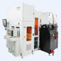
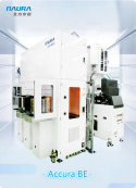
Recently, North Huachuang officially released the 12-inch plasma etching machine Accura BE, which is applied to the Bevel Etch process, achieving a "zero" breakthrough in domestic Bevel Etch equipment and contributing to my country's advanced chip manufacturing volume. Tailor-made high-efficiency solutions for yield improvement.
Thank you for the detailed and in-depth translation!Very nice.
In June 2023, North Huachuang officially released the 12-inch adhesive remover ACE i300, opening up a new territory in the field of 12-inch etching.
As a kind of etching process, the stripping process is an important link in the wafer manufacturing process. Whether the photoresist can be removed after the pattern replication and transfer is completed will directly affect whether the subsequent process can be carried out, and even related to the device. performance.
ACE i300 is mainly used in the stripping process of 12-inch storage, logic, image sensor and other fields. With excellent performance, it can realize post etch strip, post implant strip, strip Full coverage of adhesive removal processes such as descum and surface treatment.
View attachment 115313
Recently, North Huachuang officially released the 12-inch plasma etching machine Accura BE, which is applied to the Bevel Etch process, achieving a "zero" breakthrough in domestic Bevel Etch equipment and contributing to my country's advanced chip manufacturing volume. Tailor-made high-efficiency solutions for yield improvement.
View attachment 115314
- Status
- Not open for further replies.
