Chinese semiconductor industry

Status
Not open for further replies.

tokenanalyst

Brigadier
Registered Member
Thank you for the detailed and in-depth translation!
ACM Shanghai also offer a bevel etching tools for 3D NAND, since 2021, but those are wet tools they depend on liquid acids to etch the edges of the wafer, this Naura tool is a dry plasma tool so the etching process is probably more controllable, allowing higher number of layers, ACM says that their tools are higher performance than dry tools, which may be true because wet etching can be done in batches but probably is not as controllable as dry etching tools, so Naura entering this area is a huge step.


ACM Research Enters Bevel Etch Market to Support Emerging Process Steps in 3D NAND, DRAM and Advanced Logic Manufacturing.​

“During the chip manufacturing process, wafer edge peeling, particles and residue result in wafer edge yield loss, especially for 3D NAND, DRAM and advanced logic processes,” said David Wang, CEO of ACM Research. “We developed the ACM Bevel Etch product to reduce yield loss at the edge, which is becoming increasingly important to optimize overall process yields. This new product leverages ACM’s extensive wet processing expertise to deliver significant performance benefits compared to dry approaches, and consumes significantly reduced amounts of chemicals. In addition, with ACM’s proprietary technology, it can achieve more accurate and efficient wafer center alignment, which can enable it to deliver precise bevel etch that will enhance product yields and wafer throughput.”​

ACM’s Bevel Etch product supports a range of device types and process steps for 3D NAND etch, DRAM and advanced logic processes.

Please, Log in or Register to view URLs content!
 

FairAndUnbiased

Brigadier
Registered Member
ACM Shanghai also offer a bevel etching tools for 3D NAND, since 2021, but those are wet tools they depend on liquid acids to etch the edges of the wafer, this Naura tool is a dry plasma tool so the etching process is probably more controllable, allowing higher number of layers, ACM says that their tools are higher performance than dry tools, which may be true because wet etching can be done in batches but probably is not as controllable as dry etching tools, so Naura entering this area is a huge step.


ACM Research Enters Bevel Etch Market to Support Emerging Process Steps in 3D NAND, DRAM and Advanced Logic Manufacturing.​

“During the chip manufacturing process, wafer edge peeling, particles and residue result in wafer edge yield loss, especially for 3D NAND, DRAM and advanced logic processes,” said David Wang, CEO of ACM Research. “We developed the ACM Bevel Etch product to reduce yield loss at the edge, which is becoming increasingly important to optimize overall process yields. This new product leverages ACM’s extensive wet processing expertise to deliver significant performance benefits compared to dry approaches, and consumes significantly reduced amounts of chemicals. In addition, with ACM’s proprietary technology, it can achieve more accurate and efficient wafer center alignment, which can enable it to deliver precise bevel etch that will enhance product yields and wafer throughput.”​

ACM’s Bevel Etch product supports a range of device types and process steps for 3D NAND etch, DRAM and advanced logic processes.

Please, Log in or Register to view URLs content!
liquid etch has high chemical selectivity and high etch rates due to high etchant concentration, but the downside of isotropic etch which can undercut masks.

Not sure what the bevel edge etch significance is. Based on my reading, the wafer edge is easily contaminated by metals during interconnect formation in BEOL processing, but they need to deposit some sort of mask at the wafer bevel edge for wafer bonding purposes, and not etching the bevel means metal contamination between the bonded wafers.

Please, Log in or Register to view URLs content!
 

tokenanalyst

Brigadier
Registered Member
liquid etch has high chemical selectivity and high etch rates due to high etchant concentration, but the downside of isotropic etch which can undercut masks.

Not sure what the bevel edge etch significance is. Based on my reading, the wafer edge is easily contaminated by metals during interconnect formation in BEOL processing, but they need to deposit some sort of mask at the wafer bevel edge for wafer bonding purposes, and not etching the bevel means metal contamination between the bonded wafers.

Please, Log in or Register to view URLs content!
Exactly, looks like the contamination could affect the bonding and affect yield by creating faulted devices.
 

Weaasel

Senior Member
Registered Member
A long time ago Chinese capital investment funds tried to purchase Micron. The US government balked at it and forbade the investment. Micron has since systematically acquired ailing Asian memory businesses for a song, from Inotera in Taiwan, to Elpida in Japan, and Rexchip once again in Taiwan. They did this to prevent Chinese investors from getting access to the patents and know how required to manufacture memory chips. In most of those cases these acquisitions make zero financial sense for Micron except when seen through a lens of stifling competition. Chinese memory manufacturers were thus forced to develop their own products from scratch. For example JHICC did this by setting up a deal with Taiwanese UMC. UMC hired former workers from Inotera, which were fired when it was acquired by Micron, to design their memory products. Then Micron claimed these workers stole "their" IP and used the US government to attempt to kill JHICC by preventing them from acquiring or servicing the tools used to make memory chips. It is also pretty obvious they have been behind US government persecution of CXMT and YMTC.
So, they are now facing the music from what they sowed, huh?
 

tokenanalyst

Brigadier
Registered Member

】Fill in the blank of domestic 8-inch CMP equipment! Jingyi Microtech's IPO on the Science and Technology Innovation Board was accepted​


According to news from Jiwei.com, on July 2, the Shanghai Stock Exchange officially accepted the listing application of Beijing Jingyi Jingwei Technology Co., Ltd. (abbreviation: Jingyi Jingwei) Science and Technology Innovation Board.

According to the prospectus, Jingyijingwei is mainly engaged in the research and development, production, sales and technical services of semiconductor equipment. The main products are chemical mechanical polishing (CMP) equipment and its accessories, and provide technical services. CMP equipment achieves efficient removal of excess material on the wafer surface and global nanoscale planarization through the synergistic effect of chemical etching and mechanical grinding, and is mainly used in the field of integrated circuit manufacturing.

Through long-term cooperation, Jingyijingwei has established a deep strategic cooperative relationship with well-known domestic and foreign integrated circuit manufacturers. CMP equipment has been widely used in domestic and foreign advanced integrated circuit manufacturers such as SMIC, domestic customer A, world advanced, and UMC in the large-scale production line.

The global CMP equipment market is mainly occupied by Applied Materials of the United States and Ebara of Japan, and is in a highly monopolized state; the main domestic enterprises engaged in the CMP equipment business include the company and Huahai Qingke. Jingyi Jingwei and the CMP Division of the company's predecessor, the 45th Institute, have been committed to the research and development, industrialization and technical self-reliance of CMP equipment. In 2017, the CMP division of the company's predecessor, the 45th Institute, developed the first domestic 8-inch CMP equipment with independent intellectual property rights, and entered SMIC's production line for verification that year, filling the domestic 8-inch CMP equipment in integrated circuit manufacturing. The line runs blank.

From 2020 to 2022, Jingyi Jingwei achieved operating income of 99.8421 million yuan, 219.6614 million yuan and 505.8082 million yuan respectively, and net profits of -9.7649 million yuan, 14.1840 million yuan and 128.2437 million yuan respectively. The scale of operation and profit were both rapid. increase.

Jingyi Jingwei’s initial public offering of new shares will not exceed 71.3406 million shares, with a financing amount of 1.6 billion yuan. After deducting the issuance expenses, the funds raised in this issuance will be invested in “high-end semiconductor equipment research and development projects” and “high-end semiconductor equipment process improvement and industrialization” Project", "High-end Semiconductor Equipment R&D and Manufacturing Center Construction Project" and "Supplementary Working Capital".

Please, Log in or Register to view URLs content!

1688322354826.png
 

tokenanalyst

Brigadier
Registered Member

With a total investment of more than 3.9 billion yuan, 7 projects including Guangchu Technology Smart Sensor have started construction​


7 industrial projects participated in the intensive construction, with a planned total investment of over 3.9 billion yuan, including Guangchu Technology Smart Sensor Project, Yasheng Semiconductor Project, Smokang Technology Project, Lande Electronics LED Project, etc.

840605386710.0111439617365208.8425.jpg


Image source: Posted by Jiashan

The total investment of Guangchu Technology's smart sensor project is 120 million U.S. dollars, and the land area is 66 mu. The project has reached a cooperation with Chuhang Technology and will become Chuhang Technology's largest production base in East China after it settles down.

Yasheng Semiconductor project has a planned total investment of 300 million yuan and a land area of 30 mu. The project will produce 4,000 sets of intelligent semiconductor equipment and 1,000 sets of semiconductor cutting workbenches annually. After reaching full capacity, the annual output value is expected to exceed 500 million yuan.

The planned total investment of Smokang Science and Technology Project is 100 million U.S. dollars, with a land area of 21 mu. The annual output of the project is 600,000 pieces of semiconductor silicon substrates, 200,000 pieces of silicon targets and 1 million pieces of photomask quartz plates.

Lande Electronics LED project plans a total investment of 100 million yuan, with a land area of 16 acres. The project will produce 30 million meters of LED light strips and 300 million LED lamp beads per year. After the project is completed, the annual output value is expected to exceed 300 million yuan. (Proofreading/Jiang Yutong)


Please, Log in or Register to view URLs content!
 

tokenanalyst

Brigadier
Registered Member

Xinyecheng Intelligent Equipment received nearly 100 million yuan in round B financing for semiconductor equipment technology research and development, etc.​


Xinyecheng Intelligent Equipment announced that it has completed the B-round financing of nearly 100 million yuan. The investment was jointly led by CICC Qichen Fund and China Resources Fund, and Intertek Industrial followed the investment. The financing funds will be used for semiconductor equipment technology research and development, Market-oriented operation, supply chain capability improvement and organizational structure construction, etc.

The company focuses on precision optical inspection and precision laser processing, and serves the intelligent manufacturing of semiconductor, new display, new energy and other industries. Its main products include AOI testing equipment, image measuring instrument, laser marking equipment, laser microprocessing equipment, etc.

According to the official website of Xinyecheng Intelligent Equipment, in the semiconductor field, the company's products include lead frame AOI testing equipment, DBC/AMB AOI testing equipment, QFN package AOI testing equipment, IGBT DB AOI testing equipment, etc.
 

paiemon

Junior Member
Registered Member
So, they are now facing the music from what they sowed, huh?
Ironically Mircron was and still is among the weakest of the big multinational memory companies which had plenty of ground it could gain against SK Hynix and Samsung were it willing to invest in the Chinese market and/or work with local companies. Now basically they are becoming toxic to Chinese enterprise customers regardless of the existing restrictions which really only leaves them the consumer electronics sector. If YMTC remains on schedule for its localization, then it can satisfy China's 3D NAND market along with Samsung/Hynix. DRAM might be the last market bastion Micron holds in China, since I am not sure how viable CXMT and other's offerings are for enterprise and consumer products.
 

tokenanalyst

Brigadier
Registered Member

Wanye Enterprise: There is a wide space for domestic substitution and actively build a 1+N semiconductor equipment platform.​


Kaishitong: It has been fully verified by domestic leading enterprises that its competitive advantage is obvious

Kaishitong is the first equipment company in China to obtain verification and acceptance of 12-inch integrated circuit ion implanters with large beam currents and high-energy ion implanters. The company has continued to cultivate the industry for many years, and its product development has covered multiple application fields such as logic, storage, and power. , with core key models such as high-energy ion implantation and ultra-low temperature ion implantation equipment.

When talking about the competitive advantages of the company's ion implanter products, Zhang Changyong, deputy general manager of Kaishitong, said to Jiwei.com, "First, the products are developed in line with the development trend of the process and the needs of international customers. In ion implantation technology, particle pollution control, etc. It has great advantages in all aspects, covering the process requirements of domestic mainstream 28nm production lines, and has been fully verified by domestic leading enterprises. Low-energy and large-beam products have entered the mass production stage; second, the R&D team of Kaishitong has a high degree of fit In recent years, we have actively introduced a number of senior ion implantation process experts who have worked in chip manufacturing plants for many years, and the R&D team has continued to grow, so as to ensure the continuity of R&D and the timeliness of problem solving.”
Jiaxin Semiconductor: Become one of the largest R&D bases for integrated circuit front-end equipment in East China

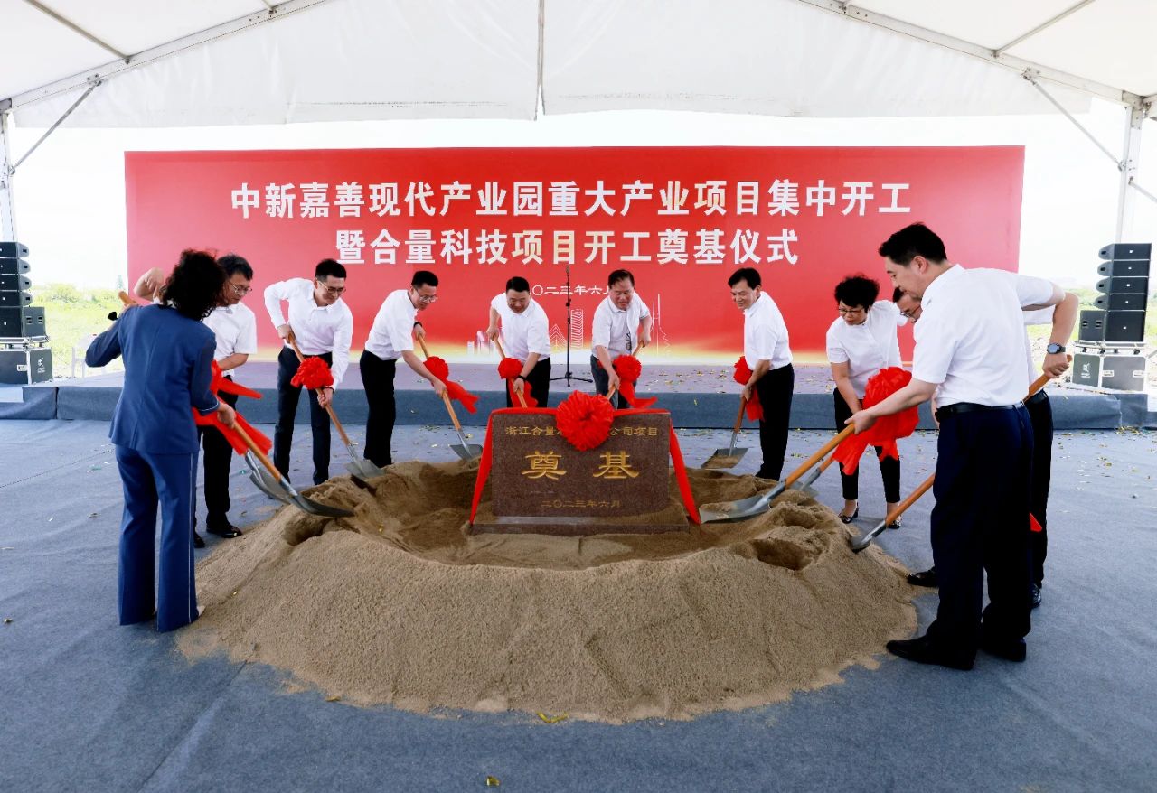
In addition to Kaishitong, Jiaxin Semiconductor, another company under Wanye Enterprise, also added strength to the localization of semiconductor equipment. According to Zhou Weifang, chairman and CEO of Jiaxin Semiconductor, Jiaxin Semiconductor was established in 2021. The 109-acre industrial park invested and built by the company completed the capping of the new factory in only 8 months. It will be moved in half a year, and will become one of the largest R&D and manufacturing bases of integrated circuit front-end equipment in East China in the future.

It is reported that the Jiaxin Semiconductor project is located in Xiadianmiao District, Xitang Town Industrial Park, Jiashan, with a total investment of 2 billion yuan, a planned area of 109 mu, and a workshop area of 140,000 square meters, covering etching machines, thin film deposition, rapid heat treatment and annealing A variety of integrated circuit core front-end equipment will form a complete equipment base in the future. Since the second half of 2022, Jiaxin Semiconductor has won multiple bids for a variety of equipment, including silicon nitride plasma etching machines, metal plasma etching machines, sidewall plasma etching machines, high-density plasma thin film deposition equipment (HDP-CVD), Silicon dioxide plasma thin film deposition equipment (PECVD), aluminum copper metal sputtering equipment (PVD), boron phosphorus doped silicon dioxide thin film chemical deposition equipment (SACVD) and titanium/titanium nitride deposition equipment (MOCVD), rapid heat treatment ( RTP) and exhaust gas treatment equipment, etc., the cumulative orders exceeded 460 million yuan.

Please, Log in or Register to view URLs content!
 
Status
Not open for further replies.
Top