
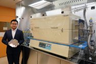
not long ago, Zhu Jiadi, a Chinese graduate student at Massachusetts Institute of Technology (MIT), broke through the successful manufacturing of atomic transistors using two-dimensional (2D) materials at room temperature. Each transistor is only three atoms thick, and the stacked chip process will easily surpass 1nm.
Currently, semiconductor chips are three-dimensional structures processed on wafers through processes such as photolithography/etching, making it very difficult to stack multiple layers of transistors for more dense integration.
Moreover, the development of advanced manufacturing processes seems to have encountered bottlenecks at 1-3nm, so many people believe that Moore's Law is over.
But semiconductor transistors made of ultra-thin 2D materials, each with a thickness of only 3 atoms, can be stacked in large quantities to create more powerful chips.
As a result, researchers at the Massachusetts Institute of Technology have developed and demonstrated a new technology that can effectively generate two-dimensional transition metal disulfide (TMD) material layers directly on silicon chips for more dense integration.
However, there is a problem with directly generating 2D materials onto silicon CMOS wafers, which is that this process typically requires a high temperature of about 600 degrees Celsius, but silicon transistors and circuits may be damaged when heated above 400 degrees Celsius.
The research achievement of Chinese graduate students such as Zhu Jiadi from the Massachusetts Institute of Technology (MIT) this time is to develop a low-temperature generation process that does not damage chips, which can directly integrate 2D semiconductor transistors onto standard silicon circuits.
In addition, this Chinese graduate student's new technology has two advantages: better craftsmanship and reduced generation time.
Previously, researchers generated 2D materials elsewhere and then transferred them onto the wafer, but this approach often resulted in defects that affected the performance of equipment and circuits, and it was also very difficult to transfer 2D materials.
In contrast, this new process will directly generate a smooth and highly uniform material layer on the entire 8-inch wafer.
Secondly, it can significantly reduce the time required to generate 2D materials. The previous method required more than a day to generate 2D materials, while the new method shortened it to within an hour.
The use of two-dimensional materials is an effective way to increase the density of integrated circuits. What we are doing is like building a multi-story building. If you only have one floor, this is the traditional situation, it won't accommodate many people. But as the floors increase, the building will accommodate more people, which can achieve amazing new things
Zhu Jiadi explained in his paper, "Due to the heterojunction integration we are studying, we use silicon as the first layer, and then we can directly integrate multi-layer 2D materials onto it
Attachments
-
 DA43859B-8F05-4F7A-B4C8-8E1FF3F302DB.jpeg162.7 KB · Views: 11

