Chinese semiconductor industry

Status
Not open for further replies.

tonyget

Senior Member
Registered Member
And again, those here would down play the significance of not having access to 3nm today, 2nm in 2025, 1.4nm in 2027. And the western expert would argue otherwise. So perhaps this is a "win-win" for both sides?? Both sides could claim victory on achieving what both sides think is important.

I think so. It's "win-win" for both,on one hand Western experts assess US sanction as a success,on the other hand it become the essential driver of Chinese semiconductor indigenization.

Just saw this new CSIS article. This is Western experts assessment "skeptical that Chinese equipment firms could supply even 5 percent of the market at the 28nm node within 3 years"

Please, Log in or Register to view URLs content!
In the equipment space, Chinese equipment firms will likely supply a majority of the new equipment for fabs producing at the 90nm node or above, according to CSIS discussions with industry executives. However, the executives were skeptical that Chinese equipment firms could supply even 5 percent of the market at the 28nm node within 3 years.

I do however,agree with some of his views,such as these:
one U.S. semiconductor executive told CSIS in an interview that the Chinese government’s actions matter less than those of the United States: “The Chinese government doesn’t even need to have a ‘no American chips’ policy,” the executive said. “The U.S. government’s actions are plenty frightening to persuade Chinese firms that they should avoid buying American unless they absolutely have to.”
In reality, China’s leading lithography company, the Shanghai Micro Electronics Equipment group (SMEE) is only producing prototype machines equivalent to what ASML was producing at scale a decade and a half ago.
 

bzhong05

New Member
Registered Member
I think so. It's "win-win" for both,on one hand Western experts assess US sanction as a success,on the other hand it become the essential driver of Chinese semiconductor indigenization.

Just saw this new CSIS article. This is Western experts assessment "skeptical that Chinese equipment firms could supply even 5 percent of the market at the 28nm node within 3 years"

Please, Log in or Register to view URLs content!


I do however,agree with some of his views,such as these:
Clearly, these experts haven't been reading Laoyaoba or other local sources... but the cognitive gap of these "analysts" and "executives" is just mind-blowing as I assumed that they would be well aware of what's going on in the global markets in spite of the language barrier. I'm just surprised that a lot of the Chinese reports on equipment or market breakthroughs never made it into the mainstream Western media.
 

tonyget

Senior Member
Registered Member
Since GAA related EDA tools was banned by the US,if Chinese fabless want to use TSMC or Samsung 3nm node,they'd probably need to use domestic EDA tools. But that could be problematic,because EDA tool makers need to work with fabs to obtain PDK,TSMC may not give GAA process info to Chinese EDA tool makers.
 

tokenanalyst

Brigadier
Registered Member
Just saw this new CSIS article. This is Western experts assessment "skeptical that Chinese equipment firms could supply even 5 percent of the market at the 28nm node within 3 years"
The article as always mostly garbage, the same sh*t on repeat, "China military...AI", "we justified because China lack this or that", "China will take a million years to get this", "Xi Bad", "SMEE ASML bla bla bla", "Unknown analyst said that or this". 5% base on what?

The manufacturing capacity of China equipment-materials makers is increasing pretty fast, going back in this threat we can see the more and more manufacturing centers for equipment, parts and materials are opening so they may be able to fill the gap way faster than these stooges think. The R&D of new equipment is accelerating as we saw with AMEC new W-CVD tool, just ACM Research Shanghai last year launched 7 types of new semiconductor equipment from a track tool, CVD, furnace and so on. Is not like this think tanker said, a new tool and that's it, there are companies launching entire family of products that complement other equipment.

Also with US monopolies out the market the competition among Chinese companies is increasing, although companies have their unique niche product, like AMEC in MOCVD and Naura in sputtering.

------------​

Ten integrated circuit projects signed and settled in Nantong, including packaging and testing equipment, etc.​


According to news from Jiwei.com, on May 11, 10 integrated circuit industry projects, including Jingxin Intelligent Headquarters and Xinyibang Semiconductor Packaging and Testing Equipment Manufacturing, signed a contract to settle in Nantong Shibei High-tech Industrial Development Zone.

It is reported that the output value of Nantong's new generation of information technology industry represented by integrated circuits has exceeded 200 billion yuan, forming a characteristic industrial system with packaging and testing as the main body, chip design, semiconductor device and equipment material manufacturing as the support. Its Chongchuan District has gathered 49 regulated integrated circuit companies such as Yutai Semiconductor, Zhisheng Microelectronics, and Yueya Semiconductor, with an output value of 30 billion yuan and a market value of nearly 100 billion yuan.

At a press conference held in April this year, Xu Wei, deputy head of Chongchuan District, said that Nantong North High-tech Zone is the forefront and main position of the development of the integrated circuit industry in Chongchuan District. First-class, create domestic first-class” development goal, high-level construction of modern integrated circuit industry demonstration zone, will make every effort to become a new landmark of Nantong integrated circuit industry. During the "14th Five-Year Plan" period, the goal of the integrated circuit industry cluster area is to attract no less than 100 new IC design companies, no less than 10 new manufacturing companies, a new industrial population of about 30,000, and an additional output value of about 300 billion. (Proofreading/Jiang Yutong)

Please, Log in or Register to view URLs content!
 
Last edited:

tphuang

Lieutenant General
Staff member
Super Moderator
VIP Professional
Registered Member
btw, last week's bids results are out. HH is still using a shockingly high amount Lam and Amat equipment in these bids
Please, Log in or Register to view URLs content!
not great, especially since these are for mature process that domestic toolmakers should have products for. I understand that domestic tool makers might not be as consistent, but it's like HH hasn't learnt any lesson from sanctions
 

Denebola

Just Hatched
Registered Member
I think so. It's "win-win" for both,on one hand Western experts assess US sanction as a success,on the other hand it become the essential driver of Chinese semiconductor indigenization.

Just saw this new CSIS article. This is Western experts assessment "skeptical that Chinese equipment firms could supply even 5 percent of the market at the 28nm node within 3 years"

Please, Log in or Register to view URLs content!


I do however,agree with some of his views,such as these:
You have to understand how western ThinkTanks work. Essentially, they are funded by political foundations very often bequeathed from the wealth of some living or dead US billionaire. Being onmessage - that's how funds are attracted, is more important than either being factual or even bothering to uncover facts, and they're also staffed by liberal arts and humanities academics. On the latter, it shows the manipulation of language and minds is of paramount concern, or they would have technical professionals with semiconductor experience combined with a knowledge of China writing these articles. The current popular Western literature that covers semiconductors and China is the 'Chip Wars' by Chris Miller. And what qualifications on the semiconductor industry does he bring to the table? None, he is an assistant Professor of international history with no prior record of writing specifically about the semiconductor industry.
As a consequence, you can discount Western opinion. They know even less than subscribers to this forum, and like previous long-running proclamations of doom about the Chinese economy as well as claims that China could not build cars or aeroengines, their opinions reflect an innate arrogance. When they're proved wrong rather than address the inadequacy of their lazy analysis, they result to the racial epithet of calling the Chinese 'sneaky' or discounting their achievements by claiming that they've stolen or copied western designs.
 

tokenanalyst

Brigadier
Registered Member
btw, last week's bids results are out. HH is still using a shockingly high amount Lam and Amat equipment in these bids
Please, Log in or Register to view URLs content!
not great, especially since these are for mature process that domestic toolmakers should have products for. I understand that domestic tool makers might not be as consistent, but it's like HH hasn't learnt any lesson from sanctions
I guess is a blind bidding process with an point based score, it would be nice to see the second and third place how far are from the first.
I still think US companies should be excluded from public biddings, although US companies are using their South East Asia subsidiaries to avoid US export controls and scrutiny.
 

tokenanalyst

Brigadier
Registered Member

Jingsheng shares: plans to invest 100 million yuan in the construction of semiconductor crystal growth equipment production and experimental projects.​


According to news from Weibo, Nanjing Jingsheng Equipment Co., Ltd. (hereinafter referred to as: Jingsheng Shares) announced on the evening of May 15 that the company intends to sign the "Project Investment Agreement" and other related supplementary agreements with the Management Committee of Nanjing Pukou Economic Development Zone. It is planned to establish a wholly-owned subsidiary Nanjing Jingcai Semiconductor Technology Co., Ltd. to invest in Nanjing Jingsheng Pukou semiconductor crystal growth equipment production and experimental projects in Pukou Economic Development Zone. The estimated total investment of the project is 100 million yuan. The project investment structure includes: carrier rental fees 10 million yuan; carrier renovation and decoration investment 20 million yuan; research and development investment 30 million yuan; production equipment and installation investment 40 million yuan.

According to the announcement, the business scope of Nanjing Jingcai Semiconductor Technology Co., Ltd. (tentative name, subject to the approval of the industrial and commercial registration authority) includes manufacturing of special equipment for semiconductor devices; sales of special equipment for semiconductor devices; research and development of special electronic materials; manufacturing of special electronic materials; Sales of materials; manufacturing of electronic special equipment; sales of electronic special equipment; sales of integrated circuit chips and products, etc.

According to the announcement, benefiting from the rapid development of the semiconductor industry, the demand for semiconductor growth equipment is rapidly released. Relying on the collaborative optimization capabilities of the upstream and downstream of the industrial chain, Jingsheng has formed its own core technology of independent research and development, and realized the deep focus of semiconductor crystal growth equipment in the semiconductor field. After the implementation of this project, it will further enhance the production capacity of Jingsheng Co., Ltd., adapt to the needs of the market, continue to promote cost reduction and increase efficiency, and enhance the company's market competitiveness.

Please, Log in or Register to view URLs content!
 

sunnymaxi

Major
Registered Member

Chinese top semiconductor equipment maker AMEC unveils its self-developed 12-inch wafer LPCVD equipment​


Advanced Micro-Fabrication Equipment Inc. China), China’s leading semiconductor equipment maker, recently launched self-developed 12-inch wafer low-pressure chemical vapor deposition (LPCVD) equipment Preforma Uniflex™ CW.

The Preforma Uniflex™ CW can flexibly configure up to five double-reactor chambers (ten reactors), and each chamber can process two wafers simultaneously. While ensuring lower production costs and chemical consumption, it achieves higher production efficiency, said the company.

The system is equipped with an optimized gas mixing scheme and heating table with independent intellectual property rights, which has excellent film uniformity, filling capacity, and process adjustment flexibility. It also has good processing capabilities for wafers with larger curvature. Its step coverage and filling capacity can meet the application requirements for contact holes and tungsten metal wires in advanced logic IC devices, DRAM, and 3D NAND, according to the company.

Please, Log in or Register to view URLs content!
 

tokenanalyst

Brigadier
Registered Member

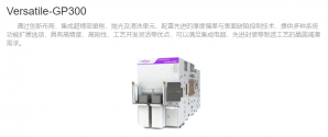
Huahai Qingke (hwatsing): Versatile-GP300 has completed the sample delivery verification of many customers, and has successively obtained sales orders. It is expected to achieve small batch shipments in 2023.​


The Versatile-GP300 of the backside thinning process of wafer has completed the sample delivery verification of many customers, and has successively obtained sales orders. It is expected to achieve small batch shipments in 2023; the 12-inch ultra-precision thinning machine for the packaging field The performance index has reached the expected goal and has been sent to the client for verification. With the application of technologies such as advanced packaging and chiplets, the market demand for thinning equipment will be greatly increased.

1684165096571.png

The self-developed cleaning equipment has been used in batches for the company's wafer regeneration production, and it is expected to be introduced to relevant market segments in 2023​


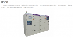
the company replied that the company's self-developed cleaning equipment It has been used in the company's wafer regeneration production in batches, and it is expected to be introduced to relevant market segments in 2023; the metal thin film thickness measurement equipment has achieved small batch shipments, and has performed well on the client side. Part of the process verification has been completed in the high-end process. Non-metallic Film thickness measurement products are also under development; HSDS/HCDS liquid supply system equipment for the supply of grinding liquid, cleaning liquid and other chemicals in wet process equipment has been purchased in batches, mainly divided into direct sales and auxiliary equipment for CMP equipment Ancillary sales, currently mainly ancillary sales.

1684165273118.png
 
Status
Not open for further replies.
Top