Chinese semiconductor industry

Status
Not open for further replies.

tokenanalyst

Brigadier
Registered Member

Xinweiyuan's 1 billion yuan high-power blue light semiconductor laser project settled in Wuhan.​


According to the "South Optics Valley" public account, on May 12, Xinweiyuan signed a contract with Jiangxia Economic Development Zone and Jiangxia Science and Technology Investment Group for the industrialization project of high-power blue light semiconductor lasers.

It is reported that the project was built by Wuhan Xinweiyuan Electronic Technology Co., Ltd. with an investment of 1 billion yuan. This project is engaged in the design and technology development of blue-ray high-power optical semiconductor laser related materials, chips, packaging, etc., as well as product research and development, manufacturing and sales. Insufficient research and development and production, to solve my country's "stuck neck" and security issues in the industrial chain, to achieve domestic substitution and independent controllable blue light semiconductor lasers.

According to public information, Wuhan Xinweiyuan Electronic Technology Co., Ltd. belongs to the laser and intelligent manufacturing industry and was established in June 2022. The company is committed to the design, research and development, production and sales of blue-ray laser materials, chips, packaging and related products (IDM full-chain business), and realizes the industrialization of domestic blue-ray lasers.

Please, Log in or Register to view URLs content!
 

tokenanalyst

Brigadier
Registered Member

Dongfang Jingyuan was invited to present the latest achievements in the first EDA International Symposium ISEDA​

Great interest for the computational lithography software PanGen and PanSim, the strict lithography simulation software of Dongfang Jingyuan. Through exchanges, everyone gained a deeper understanding of related technologies and the latest research and development progress, and at the same time, Dongfang Jingyuan The achievements achieved are highly praised and recognized.

In the forum session, Dr. Shi Weijie, executive deputy general manager of Orient Crystal, delivered a keynote speech entitled "Holistic Insights and Practices from RTL to GDS to Good Chips", which once again attracted widespread attention. At the beginning of the speech, Dr. Shi Weijie first analyzed the pain points of industry development and the challenges faced, that is, with the shrinking of feature size, the information gap between design and manufacturing links is getting bigger and bigger, resulting in a sharp increase in cost and R&D cycle. Various DTCO solutions that have emerged in recent years all attempt to repair hot spots in the manufacturing process through limited local design changes, which have certain limitations.

In his speech, Dr. Shi Weijie shared a system-level solution of Dongfang Jingyuan-Holistic Process Optimization (HPOTM), which involves manufacturability-aware physical design, OPC based on design timing, and timing critical path and Wafer defect inspection under the guidance of process hotspots. According to Dr. Shi Weijie, the completed experiments prove that the above-mentioned full-chip DTCO is greatly improved compared with previous solutions. At the end of the speech, the audience had a more detailed exchange and discussion with Dr. Shi Weijie.

Please, Log in or Register to view URLs content!
 

FairAndUnbiased

Brigadier
Registered Member

Dongfang Jingyuan was invited to present the latest achievements in the first EDA International Symposium ISEDA​

Great interest for the computational lithography software PanGen and PanSim, the strict lithography simulation software of Dongfang Jingyuan. Through exchanges, everyone gained a deeper understanding of related technologies and the latest research and development progress, and at the same time, Dongfang Jingyuan The achievements achieved are highly praised and recognized.

In the forum session, Dr. Shi Weijie, executive deputy general manager of Orient Crystal, delivered a keynote speech entitled "Holistic Insights and Practices from RTL to GDS to Good Chips", which once again attracted widespread attention. At the beginning of the speech, Dr. Shi Weijie first analyzed the pain points of industry development and the challenges faced, that is, with the shrinking of feature size, the information gap between design and manufacturing links is getting bigger and bigger, resulting in a sharp increase in cost and R&D cycle. Various DTCO solutions that have emerged in recent years all attempt to repair hot spots in the manufacturing process through limited local design changes, which have certain limitations.

In his speech, Dr. Shi Weijie shared a system-level solution of Dongfang Jingyuan-Holistic Process Optimization (HPOTM), which involves manufacturability-aware physical design, OPC based on design timing, and timing critical path and Wafer defect inspection under the guidance of process hotspots. According to Dr. Shi Weijie, the completed experiments prove that the above-mentioned full-chip DTCO is greatly improved compared with previous solutions. At the end of the speech, the audience had a more detailed exchange and discussion with Dr. Shi Weijie.

Please, Log in or Register to view URLs content!
They are manufacturer of CD SEM, now moving into EDA? I can see the synergies between simulation software and physical measurements though I don't know enough about this.
 

tokenanalyst

Brigadier
Registered Member

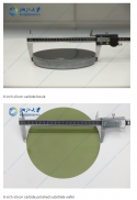
New results! The development of 8-inch conductive silicon carbide was successful​


Zhejiang University Hangzhou International Science and Technology Innovation Center (referred to as the Science and Technology Center) Advanced Semiconductor Research Institute-Hangzhou Qianjing Semiconductor Joint Laboratory (referred to as the Joint Laboratory) has recently undergone a series of technical breakthroughs in the growth of large-scale silicon carbide (SiC) single crystals and their A breakthrough has been made in substrate preparation. An 8-inch n-type silicon carbide single crystal ingot with a thickness of 27 mm has been successfully grown, and an 8-inch silicon carbide substrate sheet has been processed. It has successfully entered the 8-inch silicon carbide club. This technological breakthrough is expected to be significant Reduce the cost of silicon carbide power devices and help the development of semiconductor silicon carbide industry.

1684185777569.png

Please, Log in or Register to view URLs content!
 

hvpc

Junior Member
Registered Member
They are manufacturer of CD SEM, now moving into EDA? I can see the synergies between simulation software and physical measurements though I don't know enough about this.
indeed, they went from no EDA product to having a suite of product seemingly over night.

ASML is accusing them of IP theft.

I’m not taking I by sides, but the situation is rather suspicious.

Please, Log in or Register to view URLs content!
 

tphuang

Lieutenant General
Staff member
Super Moderator
VIP Professional
Registered Member
btw, unverified rumor at the moment so let's not spread this too much, but just another weibo account talking about HW/Hisilicon progress. Guys, no chance this is produced by HW or TSMC, so make your own conclusions

Please, Log in or Register to view URLs content!
from 定焦数码
下半年,昇腾鲲鹏天罡巴龙都会回来,麒麟旗舰芯会晚点,不是今年...

据网友分享,昇腾920的性能很强,可以赶上英伟达的H100,而且可以通过昇腾920看到麒麟回归的基本技术路线。
tips:全国在建的国产数据中心有70%采用的华为昇腾芯片... 还有 昇腾910芯片,比同期的英伟达AI芯片强,后面台积电不准代工才慢慢淡出视野
[吃瓜]
(tips部分 消息来自中国芯吧 )

Please, Log in or Register to view URLs content!
s_bcde8379e6d6412fb051e57bb7a6d765.png

I already posted this earlier, but now another prominent weibo sort of tech account is posting this

If you think that Ascend 920 being comparable in performance to H100 is a stretch, just consider that BR100 also got comparable performance to H100 using 7nm process. Except in this case, I doubt Ascend 920 will be limited by data transfer limitations facing H800 and BR100.

And I would say that 70% of China's data center using Ascend GPUs is not a stretch (based on citic securities research). There are 1.5 million Ascend developers in China. Sooner or later, China needs to ban Cuda and Nvidia GPUs and have everyone use domestic GPUs
 

tphuang

Lieutenant General
Staff member
Super Moderator
VIP Professional
Registered Member
does anyone know who these guys are?
芯盛智能
Please, Log in or Register to view URLs content!
芯盛智能发布基于RISC-V开源架构主控芯片的高性能PCIe SSD——EP2000Pro、MP2000Pro及EP3000,其还全面兼容国产自研操作系统、CPU等平台。


从官方公布的数据看,EP2000Pro搭载XT8111V110主控,采用3D TLC NAND,具备PCIe3.0×4高速接口,支持NVMe1.4协议,顺序读写高达3500/3300MBps,4K随机读写可达237K/600K IOPS,MTBF 150万小时,运行功耗≤4w,空闲功耗≤0.5w,容量从256GB-2TB均有覆盖,兼容国产平台。
this seems like RISC-V based control chip for SSD. Makes sense you would need a chip for that. But does anyone know if these numbers of 3500/3300MBps are competitive? IIRC, YMTC SSDs have higher I/O speed than this. Wouldn't control chip limitations be a problem? I have no idea what other SSDs use. I'm assuming this comes with the NAND itself

EP3000搭载基于RISC-V开源架构的XT8210V100主控,采用3D TLC NAND,具备PCIe4.0 x 4高速接口,支持NVMe1.4协议,顺序读写高达5000/4700MBps。


此外,其4K随机读写可达650K/700K IOPS,MTBF 150万小时,运行功耗≤4w,空闲功耗≤0.5w,容量从512GB~2TB均有覆盖,同样兼容国产平台。
oh, actually EP3000 seems better and able to handle the I/O of YMTC's newer SSDs
 

FairAndUnbiased

Brigadier
Registered Member
indeed, they went from no EDA product to having a suite of product seemingly over night.

ASML is accusing them of IP theft.

I’m not taking I by sides, but the situation is rather suspicious.

Please, Log in or Register to view URLs content!
the original case was against XTAL which is alleged to steal OPC software.

Please, Log in or Register to view URLs content!

so the question is, how closely related is Dongfang's tech to OPC?

I think so. It's "win-win" for both,on one hand Western experts assess US sanction as a success,on the other hand it become the essential driver of Chinese semiconductor indigenization.

Just saw this new CSIS article. This is Western experts assessment "skeptical that Chinese equipment firms could supply even 5 percent of the market at the 28nm node within 3 years"

Please, Log in or Register to view URLs content!


I do however,agree with some of his views,such as these:

lol they are political 'scientists' not semiconductor scientists.
 

coolieno99

Junior Member
Usually Youtube videos are poor sources for information on the development on China's EUV lithography tool. But the following video is an exception. And it is believable. The narrator mention the accurracy of positioning of the dual stage table is measure in units of pm. I assume pm means picometer, or 1/1000 of nanometer. But I am not sure.


From the info given in this video, it looks like China can/will ship out a production ready EUV lithography tool before or in 2025.
 
Status
Not open for further replies.
Top