Chinese semiconductor industry

Status
Not open for further replies.

tokenanalyst

Brigadier
Registered Member

The mass-produced model of Microchip solar cell lithography equipment was successfully shipped​

Please, Log in or Register to view URLs content!


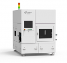
In April 2023, the mass-produced model (SDI-15H) of Microchip Solar Cell Lithography Equipment was successfully shipped to leading photovoltaic companies. The equipment shipped this time is an upgraded model of the first micro-mounted solar cell lithography equipment in September 2022, which is suitable for mass production applications of high-efficiency solar cell lithography patterning processes.

SDI-15H solar cell lithography equipment has broad application prospects in new photovoltaic cell processes such as heterojunction cell (HJT) copper plating, XBC solar cell and so on. Microchip direct writing lithography technology provides a new high-precision and low-cost graphics solution for the photovoltaic industry to reduce costs and increase efficiency, and solve the pain points of high-efficiency solar cell industrialization.
1682394931541.png

The SDI-15H solar cell lithography equipment of Xinqi Micro Devices adopts advanced digital lithography technology, which can directly transfer complex and high-precision patterns to the surface of solar cells without a mask. Produce the first application. SDI-15H solar cell direct writing lithography system adopts multi-optical engine parallel scanning technology, with high-precision analysis (15μm+), high-precision pattern alignment (<10μm), high-speed processing capability (single track ≥ 6000 half-chip/hour), etc. performance, and the processing process has the advantages of no contact, no pollution, no laser damage, no mask consumption, etc.

Under the background that "carbon neutrality" has become a global consensus, and green renewable energy has gradually become the mainstream of future energy in the world, vigorously developing photovoltaic green energy is an important way to realize the sustainable development of human energy. Grasping the pulse of the development of the times, Xinqi Microdevice will continue to promote the wide application of direct writing lithography technology in the field of green energy, and realize the corporate vision of "world brand of IC equipment".

Please, Log in or Register to view URLs content!
 

FairAndUnbiased

Brigadier
Registered Member

The mass-produced model of Microchip solar cell lithography equipment was successfully shipped​

Please, Log in or Register to view URLs content!


In April 2023, the mass-produced model (SDI-15H) of Microchip Solar Cell Lithography Equipment was successfully shipped to leading photovoltaic companies. The equipment shipped this time is an upgraded model of the first micro-mounted solar cell lithography equipment in September 2022, which is suitable for mass production applications of high-efficiency solar cell lithography patterning processes.

SDI-15H solar cell lithography equipment has broad application prospects in new photovoltaic cell processes such as heterojunction cell (HJT) copper plating, XBC solar cell and so on. Microchip direct writing lithography technology provides a new high-precision and low-cost graphics solution for the photovoltaic industry to reduce costs and increase efficiency, and solve the pain points of high-efficiency solar cell industrialization.

View attachment 111557

The SDI-15H solar cell lithography equipment of Xinqi Micro Devices adopts advanced digital lithography technology, which can directly transfer complex and high-precision patterns to the surface of solar cells without a mask. Produce the first application. SDI-15H solar cell direct writing lithography system adopts multi-optical engine parallel scanning technology, with high-precision analysis (15μm+), high-precision pattern alignment (<10μm), high-speed processing capability (single track ≥ 6000 half-chip/hour), etc. performance, and the processing process has the advantages of no contact, no pollution, no laser damage, no mask consumption, etc.

Under the background that "carbon neutrality" has become a global consensus, and green renewable energy has gradually become the mainstream of future energy in the world, vigorously developing photovoltaic green energy is an important way to realize the sustainable development of human energy. Grasping the pulse of the development of the times, Xinqi Microdevice will continue to promote the wide application of direct writing lithography technology in the field of green energy, and realize the corporate vision of "world brand of IC equipment".

Please, Log in or Register to view URLs content!
more development direct write litho could potentially mean cabbagization of analog, power and optoelectronic chips. bad news for certain companies.
 

tokenanalyst

Brigadier
Registered Member

Boyang Microelectronics Tongling ultra-high-purity wet electronic chemicals project is expected to be put into operation in June next year​


Tongling released news that Boyang Microelectronics (Tongling) Co., Ltd., located in Tongling Economic Development Zone, Anhui Province, has an annual output of 100,000 tons of ultra-high-purity wet electronic chemicals project officially started in March this year, and is currently under pile foundation. Construction is expected to be put into production in June next year.

The total investment of the project is 1.05 billion yuan. After completion, high-purity isopropanol at the G5 international standard level will be produced. The products basically realize the import substitution of high-purity chemical reagents. They are mainly used in lithography, development, etching, Stripping, cleaning and other production processes.

Tianyan Check shows that Boyang Microelectronics (Tongling) Co., Ltd. was established in August 2022 and is 100% owned by Suzhou Boyang Chemical Co., Ltd.

In August 2022, the semiconductor and optical electronic material project of Suzhou Boyang Chemical Co., Ltd. signed a contract and settled in Tongling Economic and Technological Development Zone, Anhui. On November 18 of the same year, Boyang Microelectronics (Tongling) Co., Ltd. held a foundation laying ceremony in Tongling Economic and Technological Development Zone. According to the news at the time, Wang Guohong, chairman of Boyang Co., Ltd., said that high-purity isopropanol will meet the international G5 standard in the Tongling factory, and will serve 8-inch and 12-inch wafer manufacturing and semiconductor packaging and testing in the future.

Please, Log in or Register to view URLs content!
 

tokenanalyst

Brigadier
Registered Member

Jiuri New Materials: Dajing Information's special photosensitizer PAC for photoresist has been supplied in small batches​


recently, an investor asked a question on the investor interaction platform: Please update the photoresist sample delivery status of your company Jiuri Semiconductor and Dajing Information. The previous reply has been produced in small batches. Is there any new sample delivery or There is a new certification progress, small batch to mass production?

Jiuri New Materials (688199.SH) stated on the investor interaction platform on April 25 that as of now, Jiuri Semiconductor has completed the research and development of a variety of semiconductor i-line photoresist formulations, and the test performance indicators are completely comparable to those in the domestic market. Imported products are comparable, and the sample delivery verification work for key customers and the construction of pilot production lines are underway; Dajing Information’s photoresist special photosensitizer PAC has completed sample delivery to eleven downstream companies, and has begun to send small batches to some companies Supply.

As of press time, the market value of Jiuri New Materials is 3.39 billion yuan, and the stock price is 30.48 yuan per share, down 4.6% from the closing price of the previous day.

Please, Log in or Register to view URLs content!
 

huemens

Junior Member
Registered Member

SK Hynix to postpone completion of new NAND plant in China, likely to sell it directly​

Please, Log in or Register to view URLs content!

SK Hynix will postpone the completion of its second NAND plant in Dalian, northeastern China, and is also likely to directly sell the plant after the completion before installing manufacturing equipment, according to reports from Korean news media
 

tokenanalyst

Brigadier
Registered Member

The prosperity of the semiconductor equipment industry continues, and Xinyuanwei’s (KingSemi) net profit in the first quarter increased by 103.55% year-on-year​


Jiwei.com reported that on April 25, Xinyuan Micro released the first quarter report of 2023, stating that the company’s revenue in the first quarter was 288 million yuan, a year-on-year increase of 56.89%; net profit was 65.9774 million yuan, a year-on-year increase of 103.55%.

Xinyuanwei said that the company's revenue growth was mainly due to the continued prosperity of the semiconductor equipment industry and the company's revenue scale continued to grow. The increase in net profit was mainly due to the increase in the company's sales revenue and the increase in tax rebates for embedded software products during the reporting period. .

According to the data, Xinyuanwei is mainly engaged in the research and development, production and sales of special equipment for semiconductors. Glue machine, wet etching machine), which can be used for 8/12-inch single wafer processing (such as front-end wafer processing and back-end advanced packaging in integrated circuit manufacturing) and 6-inch and below single-wafer processing (such as compound, MEMS, LED chip manufacturing, etc.).
 

tphuang

Lieutenant General
Staff member
Super Moderator
VIP Professional
Registered Member

SK Hynix to postpone completion of new NAND plant in China, likely to sell it directly​

Please, Log in or Register to view URLs content!
interesting. looks like YMTC can buy something really cheap. I was wondering where YMTC's next plant would be. Dalian would make sense

okay here is the english translation of the korean article
Please, Log in or Register to view URLs content!

Quite interesting. Looks like a pretty good choice here for YMTC. There must be a lot of people already in Dalian capable of filling the positions. YMTC also would not need to negotiate for land or anything With Dalian gov't. I'm sure Dalian gov't would gladly see YMTC filling in here. Good opportunity. Just need domestic SMEs to be able to supply the equipments to ramp up production.
 
Last edited:

tokenanalyst

Brigadier
Registered Member
more development direct write litho could potentially mean cabbagization of analog, power and optoelectronic chips. bad news for certain companies.
For now mask lithography (even SMEE 300 series) still have the advantage of higher resolution-throughput against laser, slm, dmd litho systems but for how long that is the question. SMEE should push for the commercialization of their frontend scanners and there should be more enforcement on their use.
 

huemens

Junior Member
Registered Member
interesting. looks like YMTC can buy something really cheap. I was wondering where YMTC's next plant would be. Dalian would make sense

okay here is the english translation of the korean article
Please, Log in or Register to view URLs content!

Quite interesting. Looks like a pretty good choice here for YMTC. There must be a lot of people already in Dalian capable of filling the positions. YMTC also would not need to negotiate for land or anything With Dalian gov't. I'm sure Dalian gov't would gladly see YMTC filling in here. Good opportunity. Just need domestic SMEs to be able to supply the equipments to ramp up production.

What about CXMT. They are planning an IPO.
 

huemens

Junior Member
Registered Member

Chinese-owned Nexperia BV has asked ATREG Inc. to help it sell its wafer fab in Newport, Wales, in compliance with UK government instructions.​

Please, Log in or Register to view URLs content!

In its 1Q23 newsletter ATREG said it “looks forward to working with Nexperia regarding its operational, automotive-qualified 200mm manufacturing facility located in Newport, South Wales, which is the UK’s largest semiconductor site spanning 28 acres (12 hectares).”

In the newsletter ATREG provided some details of the fab campus: a ballroom cleanroom facility built in 1998 suitable for 200mm-diameter wafers, with accompanying test area. The site also includes a 150mm wafer modular cleanroom. “With proper investments, the site can also be used for production of compound semiconductors,” ATREG said.

The fact that ATREG has been engaged does not mean a sale is necessarily imminent and Nexperia could still be pursuing is judicial review of the UK government’s decision.
 
Status
Not open for further replies.
Top