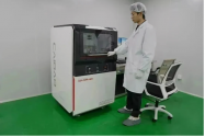
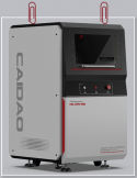
Caidao self-developed the first 12-inch industrial-end wafer-level atomic force microscope in China.
Caidao Precision is the first company in China to have an all-round layout of "precision ultra-precision industrial microscopic equipment", mainly focusing on the semiconductor and pan-semiconductor industries. Under the background of "US core ban", "low localization rate of semiconductor equipment" and "domestic substitution is imperative", Caidao will actively deploy the field of semiconductor measurement equipment in 2019 to meet the advanced process capacity of domestic semiconductor large silicon wafers Opportunities to expand are coming.
After more than three years of hard work, in March 2023, Caidao launched the domestic "industrial end" 12-inch wafer-level atomic microscope (nano microscope), filling the gap in the domestic industry. This equipment is one of the indispensable equipment for measuring the roughness and key dimensions of semiconductors, pan-semiconductor materials and devices, especially in the advanced process of semiconductors below 28 nanometers, the supply of measurement equipment is almost blank in China. Caidao Precision launched a 12-inch wafer-level atomic force microscope. For the semiconductor equipment industry, domestic substitution is of great significance.
The measurement accuracy of the 12-inch wafer-level atomic force microscope is at the nanometer level, the XY axis can reach 0.3 nanometers, and the Z axis can reach 0.035 nanometers. The scanning speed is greatly improved, and the scanning speed of each picture is 20-50 seconds, which is much higher than the usual scanning speed of 5-8 minutes. There are also many advantages such as one-button opening, automatic film change, automatic needle insertion, and dual-screen display. Please call us for details.
The successful development of the atomic force microscope has enabled Caidao’s precision microscopic inspection equipment to complete the complete layout from micron, submicron, to nanometer. The company originally had detection and measurement equipment, and through integration, the detection accuracy can be improved to the nanometer level.
View attachment 110999View attachment 111000


