Peking University reported an epitaxial high-κ gate dielectric integrated two-dimensional fin transistor.
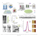
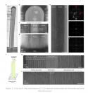
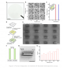
the research group of Professor Peng Hailin of Peking University published a research paper entitled "2D fin field-effect transistors integrated with epitaxial high-κ gate oxide" in the journal Nature .This study reported a new two-dimensional semiconductor vertical fin/high dielectric self-oxide epitaxial integration architecture (2D fin/oxide Bi 2 O 2 Se/Bi 2 SeO 5 ), and developed a high-performance two-dimensional fin field Effect Transistor (2D FinFET). The two-dimensional semiconductor fin/self-oxide epitaxial heterostructure has an atomically flat interface and an ultra-thin fin thickness (up to a unit cell thickness, ~1.2 nm), and realizes the wafer-level single-directional array preparation and fixed-point , high-density growth. Two-dimensional FinFETs based on Bi2O2Se/Bi2SeO5epitaxial heterojunctions have highelectron mobility up to 270 cm 2 /Vs, extremely low off-state current (~1 pA/μm) and very High on/off current ratio (10 8 ), the on-state current density is as high as 830 μA/μm when the channel length is 400 nm, meeting the 2028 low-power device target requirements of the International Device and System Roadmap (IRDS). This original work broke through the bottleneck of three-dimensional heterogeneous integration of key new materials and new architectures for high-speed and low-power chips in the post-Moore era, and brought new opportunities for the development of future chip technologies that break through the limits of silicon-based transistors.


