Chinese semiconductor industry

Status
Not open for further replies.

luminary

Senior Member
Registered Member

Trade Minister, SK hynix CEO says
Please, Log in or Register to view URLs content!


SK hynix vice-chair and co-CEO Park Jung-ho yesterday
Please, Log in or Register to view URLs content!
told his annual shareholder meeting yesterday that the chip shop considered applying for CHIPS Act funding, though complained: "We found the process too demanding."

The US last week
Please, Log in or Register to view URLs content!
it would ease the latter concerns, by allowing chipmakers with existing Chinese facilities to expand them by up to ten percent – double the previously-touted five percent limit.

Park also told the meeting that SK hynix is reviewing all its investments amid
Please, Log in or Register to view URLs content!
for semiconductors.

South Korea has passed legislation giving tax breaks to its semiconductor companies in a bill being labelled as the "Korean Chips Act." At the same time, the nation's trade minister repeated its complaints that the criteria for Korean companies to access US funding are unpalatable in a possible sign of growing protectionism in the worldwide chip market.

Please, Log in or Register to view URLs content!
 

tphuang

Lieutenant General
Staff member
Super Moderator
VIP Professional
Registered Member
AMEC first Epitaxial deposition equipment after 18 months of development. A record time for the company.

View attachment 110136

(4) Research and development of thin film deposition equipment During the reporting period, the company's first CVD tungsten
equipment was delivered to key storage clients for verification and evaluation.

Prior to this, CVD tungsten had completed stability tests and customer test verification in the laboratory, and it was applied to metal interconnection. The performance of CVD tungsten process equipment has been able to meet the needs of customers for process verification. At the same time, the company is verifying CVD tungsten equipment with more logic and storage customers, and has made a number of progresses to lay the foundation for further accumulation of market advantages. On the basis of metal tungsten CVD equipment, the company is further developing new types of CVD tungsten and ALD tungsten equipment to achieve material filling of higher aspect ratio structures. New types of CVD tungsten and ALD tungsten equipment are key equipment for high-end storage devices. Currently Laboratory testing has begun and key customers have started docking verification. The ALD titanium nitride equipment developed by the company for high-end storage and logic devices is also advancing steadily and has entered the stage of laboratory testing. Based on the existing research and development of metal CVD and ALD equipment, the company plans to develop more advanced CVD and ALD equipment, increase the coverage of thin film equipment, and further expand the market.​
It seems like AMEC is making pretty good progress in ICP and CCP. I saw this. I think the good part is that it looks like they have all the 28nm process covered now and that's good.
1.研发:2022年报关于产品和研发的篇幅相比前两年大幅增加,对于我这种外行人员来说受益匪浅。CCP的大马士革和极高深宽比明面意思是开发出设备了,我估计性能和可靠性还需要再优化和验证,所以没有公布对应的型号;ICP公布了几个新的子设备型号,面对成熟工艺产品刻蚀机系列已经完整了;LPCVD的开发速度创公司历史,后续的开发中的型号是国内半导体制造厂扩产的关键设备。2.高管国籍和人员名单在股权激励公告中提到了,基本没有变化,外籍人才引进估计国家层面也在制定政策,总不能让别人交的弃籍税多于入中(港)享受到的福利待遇吧,这个只能边走边看了。3.员工持股平台的持股量相比三季度减少了10-20%,还有大几十亿的市值,接下来看一季报吧
We know from multiple reports that de-americanized 28nm process is coming online this year with SMIC jingcheng whenever they start production. The question is whether or not their Amat/Lam replacement tools can Looks like based on the diagrams, their tools are sufficient for multi-pattern, which means they can be used for 12/14nm process.

I keep asking this question the past month because it looks like they are getting to the point where they can replace Lam equipments in 12/14nm process. In yours and @PopularScience posts, it look like their equipment can be used in sub 28nm process. In fact, his attached photos explicitly says so. It also talks about high aspect ratio etcher that can be used in 3D NAND production unless I'm reading it incorrectly.

This seems to confirm the expectations that their tools will allow YMTC to continue their 128-layer production. It also seems to indicate to me they can replace Lam in at multi-patterning at least at 12/14nm process. I'm not saying this will achieve same level of yield as using American tools, but they don't particularly have any choices here. That to me seems to be enough for SMIC to expand 12/14nm process. What do you think @FairAndUnbiased @hvpc?
 

siegecrossbow

General
Staff member
Super Moderator
It seems like AMEC is making pretty good progress in ICP and CCP. I saw this. I think the good part is that it looks like they have all the 28nm process covered now and that's good.

We know from multiple reports that de-americanized 28nm process is coming online this year with SMIC jingcheng whenever they start production. The question is whether or not their Amat/Lam replacement tools can Looks like based on the diagrams, their tools are sufficient for multi-pattern, which means they can be used for 12/14nm process.

I keep asking this question the past month because it looks like they are getting to the point where they can replace Lam equipments in 12/14nm process. In yours and @PopularScience posts, it look like their equipment can be used in sub 28nm process. In fact, his attached photos explicitly says so. It also talks about high aspect ratio etcher that can be used in 3D NAND production unless I'm reading it incorrectly.

This seems to confirm the expectations that their tools will allow YMTC to continue their 128-layer production. It also seems to indicate to me they can replace Lam in at multi-patterning at least at 12/14nm process. I'm not saying this will achieve same level of yield as using American tools, but they don't particularly have any choices here. That to me seems to be enough for SMIC to expand 12/14nm process. What do you think @FairAndUnbiased @hvpc?

What does CCP stand for in the context of semiconductors? I know PLA is programmable logic array.
 

tphuang

Lieutenant General
Staff member
Super Moderator
VIP Professional
Registered Member
Please, Log in or Register to view URLs content!
Again, says that it has received multiple (repeat) orders of its etching tools in 5nm & next gen process (I assume this is for a less critical part of the process)

Probably just as important, it has a new facility in Nanchang that went into production in July of last year that is 140k sqm. It will have another new facility in Shanghai Lingang that's 180k sqm that will start production this year. So, huge expansion plans for AMEC.

it's developing MOCVD for Micro-LED for high end displays. It's also developing tools for producing GaN and Silicon Carbide power devices.
 

olalavn

Senior Member
Registered Member
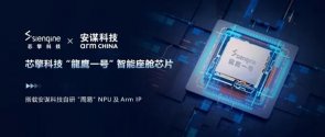
Hubei Xinqing Technology announced that China's first 7nm automotive-grade SoC chip "Longying No. 1" has been mass-produced and supplied

It is reported that the Longying No. 1 positioning smart cockpit chip adopts ARM CPU/GPU and ARM Technology (China) self-developed "Zhouyi" NPU architecture design, integrates 87 layers of circuits, and has 8.8 billion transistors. In addition, it also integrates VPU, ISP, DPU, and DSP clusters, and has a built-in information security engine that complies with national secret algorithms and a safety island design that complies with ASIL-D standards.

Other disclosed specifications include 8-core CPU, 14-core GPU, support for LPDDR5-6400 memory, 8 TOPS AI computing power, 0.9T GPU floating-point computing power, etc.

640 (1).jpg640.jpg
 

FairAndUnbiased

Brigadier
Registered Member
It seems like AMEC is making pretty good progress in ICP and CCP. I saw this. I think the good part is that it looks like they have all the 28nm process covered now and that's good.

We know from multiple reports that de-americanized 28nm process is coming online this year with SMIC jingcheng whenever they start production. The question is whether or not their Amat/Lam replacement tools can Looks like based on the diagrams, their tools are sufficient for multi-pattern, which means they can be used for 12/14nm process.

I keep asking this question the past month because it looks like they are getting to the point where they can replace Lam equipments in 12/14nm process. In yours and @PopularScience posts, it look like their equipment can be used in sub 28nm process. In fact, his attached photos explicitly says so. It also talks about high aspect ratio etcher that can be used in 3D NAND production unless I'm reading it incorrectly.

This seems to confirm the expectations that their tools will allow YMTC to continue their 128-layer production. It also seems to indicate to me they can replace Lam in at multi-patterning at least at 12/14nm process. I'm not saying this will achieve same level of yield as using American tools, but they don't particularly have any choices here. That to me seems to be enough for SMIC to expand 12/14nm process. What do you think @FairAndUnbiased @hvpc?
My opinion is that this means they've developed good supply chain cleanliness requirements and have mastered the secrets of semiconductor etch: 1. heater design 2. gas supply design 3. chamber coatings

14 nm vs 28 nm is not that big of a difference for etching. But there's a few differences. 1. the overall chemical resistance requirements get stricter and stricter for plasma facing components and 2. the heater uniformity requirements are extremely high.

Please, Log in or Register to view URLs content!

Remember that temperature is exponentially related to reaction rate, and while it doesn't matter for larger scales, at <20 nm scales, even a 0.1 degree C difference in temperature uniformity can mean a +/- a few nm in dimensions... which for a 10 nm CD structure is a 20-30% deformation.


Lam_Research_Figure_02-1024x749.jpg

Please, Log in or Register to view URLs content!

Finally, the etch gas delivery system has to deliver absolute uniformity as well at lowest cost.

Lam_Research_Figure_01-788x1024.jpg
 

FairAndUnbiased

Brigadier
Registered Member
Will I be forced, by the power vested in me as SDF moderator, to declare that chipmaking is a junk tier technology easily mastered by any nation within the next five years?
you need to declare CCP, aka DA SEE SEE PEE, is an evil totalitarian process that must be forever banned from democratic All Murican Made in the US of A Red White and Blue fabs.
 
Status
Not open for further replies.
Top