You are using an out of date browser. It may not display this or other websites correctly.
You should upgrade or use an alternative browser.
You should upgrade or use an alternative browser.
Chinese semiconductor industry
- Thread starter Hendrik_2000
- Start date
- Status
- Not open for further replies.
Beijing University of Science and Technology's "Key Laboratory of Key New Materials and Devices for Chips in the Post-Moore Era" was approved for construction by the Ministry of Education
According to the official Weibo news of Beijing University of Science and Technology, recently, the Ministry of Education announced the list of newly established key laboratories of the Ministry of Education in 2022. Successfully approved.
It is reported that the construction goals and key tasks of this key laboratory are to focus on two-dimensional semiconductor materials and other transformative material systems that break through the limit of size reduction, develop new methods and new equipment for the controllable preparation of wafer-level two-dimensional semiconductor materials, and establish new principles New technologies for functional coupling and system integration of low-power devices, development of new architectures for high-computing logic circuits with low-generation processes equivalent to advanced processes, and development of new materials and devices for advanced processes in the post-Moore era that are compatible with silicon-based CMOS processes The technical route is to create a cutting-edge cross-research platform with deep integration of multiple disciplines, a high level, and a full chain, and to establish a Chinese track for advanced chips in the post-Moore era, breaking the dilemma that China's chip technology has long been controlled by others.
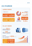
AMEC first Epitaxial deposition equipment after 18 months of development. A record time for the company.
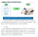


(4) Research and development of thin film deposition equipment During the reporting period, the company's first CVD tungsten
equipment was delivered to key storage clients for verification and evaluation.
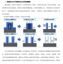
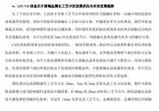
Prior to this, CVD tungsten had completed stability tests and customer test verification in the laboratory, and it was applied to metal interconnection. The performance of CVD tungsten process equipment has been able to meet the needs of customers for process verification. At the same time, the company is verifying CVD tungsten equipment with more logic and storage customers, and has made a number of progresses to lay the foundation for further accumulation of market advantages. On the basis of metal tungsten CVD equipment, the company is further developing new types of CVD tungsten and ALD tungsten equipment to achieve material filling of higher aspect ratio structures. New types of CVD tungsten and ALD tungsten equipment are key equipment for high-end storage devices. Currently Laboratory testing has begun and key customers have started docking verification. The ALD titanium nitride equipment developed by the company for high-end storage and logic devices is also advancing steadily and has entered the stage of laboratory testing. Based on the existing research and development of metal CVD and ALD equipment, the company plans to develop more advanced CVD and ALD equipment, increase the coverage of thin film equipment, and further expand the market.
Tuojing Technology (Piotech) set up a subsidiary in Shanghai with 100 million yuan including sales of special equipment for semiconductor devices
Qichacha APP shows that recently, Shanghai Yanquan Technology Co., Ltd. was established with a registered capital of 100 million yuan. The business scope includes: sales of electronic special equipment; Sales of special equipment for semiconductor devices; sales of mechanical parts and spare parts, etc. Qichacha equity penetration shows that the company is 100% controlled by Tuojing Technology.
Qichacha APP shows that recently, Shanghai Yanquan Technology Co., Ltd. was established with a registered capital of 100 million yuan. The business scope includes: sales of electronic special equipment; Sales of special equipment for semiconductor devices; sales of mechanical parts and spare parts, etc. Qichacha equity penetration shows that the company is 100% controlled by Tuojing Technology.
The 12-inch wafer-level TSV stereo integration project of Xi'an Microelectronics Technology Research Institute has begun construction
SMIC: 28nm high voltage, 55nm BCD and other processes have been trial production
SMIC: 28nm high voltage, 55nm BCD and other processes have been trial production
Xi'an Microelectronics Technology Research Institute's 12-inch wafer-level TSV stereo integration project started construction.

Zhao Shijian said in his speech that the 12-inch wafer-level TSV three-dimensional integration project was launched in Zhuhai High-tech Zone, which will definitely promote the strengthening and supplementation of Zhuhai's integrated circuit industry chain, help Zhuhai break through key core technologies in the field of integrated circuits, and help promote the East to build Integrated circuit "third pole". Zhuhai High-tech Zone will provide the project with the best policy support, the best carrier supporting facilities, the best business environment, and the best talent ecology, fully support the project to become better and bigger, and jointly create a benchmark brand in the integrated circuit industry in the Greater Bay Area.
Tang Lei said in his speech that the Zhuhai 12-inch wafer-level TSV three-dimensional integration project is another important milestone to realize the deep integration of aerospace technology and market resources and build a world-class electronic technology powerhouse. With the strong coordination and close cooperation of all parties , The project will surely achieve the development goals of scale, industrialization, and clustering, and provide strong support for improving the development of the entire integrated circuit industry chain in the Guangdong-Hong Kong-Macao Greater Bay Area and promoting the high-quality development of the local economy.
Tang Lei said in his speech that the Zhuhai 12-inch wafer-level TSV three-dimensional integration project is another important milestone to realize the deep integration of aerospace technology and market resources and build a world-class electronic technology powerhouse. With the strong coordination and close cooperation of all parties , The project will surely achieve the development goals of scale, industrialization, and clustering, and provide strong support for improving the development of the entire integrated circuit industry chain in the Guangdong-Hong Kong-Macao Greater Bay Area and promoting the high-quality development of the local economy.
- Status
- Not open for further replies.

