Can someone explain the news about Huawei and 14nm Chips. Can they produce what ASML does or something when it comes to the tools used to make the machines? Frrom what I know China already knows how to make advanced chips but not the tools needed for those chips.
You are using an out of date browser. It may not display this or other websites correctly.
You should upgrade or use an alternative browser.
You should upgrade or use an alternative browser.
Chinese semiconductor industry
- Thread starter Hendrik_2000
- Start date
- Status
- Not open for further replies.
Can someone explain the news about Huawei and 14nm Chips. Can they produce what ASML does or something when it comes to the tools used to make the machines? Frrom what I know China already knows how to make advanced chips but not the tools needed for those chips.
14nm is indigenous chip design software only.
according to my news...it's Nikon...Can someone explain the news about Huawei and 14nm Chips. Can they produce what ASML does or something when it comes to the tools used to make the machines? Frrom what I know China already knows how to make advanced chips but not the tools needed for those chips.
If you want to produce the domestic 14/12/10nm process, you have to wait until 2025
Is there any news on EUV and stuff? Can someone contextualise how big this breakthrough is ?
You’ll know about big breakthrough when there is a Huawei Carl video.
There are more than three categories that analysts usually breakdown IC chips. Basic segmentations I’ve seen by the likes of IC Insight, Gartner, VLSI Research:- Just a few questions for clarity, commercial IC chips are mostly divided into three categories processor, memory, and analog chips (these are mostly single function chips like power and sound chips) right?
-Logic: I’ve seen subcategories such as Leading edge logic, advanced logic, and Mature Logic. But mostly it’s subsegmented to Advanced (anything below 40nm node) and Mature Logic (40nm node and above)
- Memory: DRAM, 3D-NAND
- Analog (anything that deals with analog signal I would put in this category. RF, PMIC are usually bucketed here)
- Optical sensors (CMOS imaging sensor)
- Non-optical sensors
- Power (IGBT, discrete, etc)
- MEMS
everything outside of logic and memory are also often referred by foundries as “speacialty applications”.
- 90/65/45/32/22/16/10/7/5/3nm are Logic design nodes. There are half-nodes that we often read about, too (e.g. 55nm half-node is usually bucketed with 65nm; 40nm with 45nm node; 12/14nm bucketed under 16nm, etc.)- Do the various nanometre nodes 90, 45, 28, 14, 10 nm apply equally to processor, memory, and analog chips?
- DRAM and Logic used to share same node convention. But this started to split off at around 22nm node. DRAM 20nm node or D20 came out sbout the same time as 20nm logic. Then subsequent DRAM nodes are designated as D1x/D1y/D1z/D1a//D1z
- Analog usually utilizes outdated logic process and equipment. Standard logic node s are used to describe varying level of analog chips. But keep in mind analog chips are not same complexity as logic. analog chips require much less patterning steps (or number of reticles) as logic. So a 45nm Logic chip is much more complex to make than say a 45nm analog chip.
I’m not aware of any IDM other than Intel that design and build their own processor chip. Maybe others can chime in. But as far as I know, CPU, MPU, GPU chips are mostly build under the fabless/foundry model.- SMIC, the most prominent maker of processor chips in China is a contract chip manufacturer, but does China have any prominent integrated device manufacturers that make processor chips?
by the way, foundries like SMIC makes everything from processors (GPU, CPU, MPU) to all specialty application chips
I can’t say for sure but it certainly looks that way. Once Huawei obtain full wafer fabrication capability to produce chips they design then by definition they could be categorized as an IDM. But I doubt they could come up with a fab in the near term that could fulfill 100% of their own chips/IC design needs. So I think it’s probably more accurate to expect Huawei to operate under a hybrid IDM - fabless model.- Is Huawei planning to be an IDM?
Its just more of the "China doomed" bullshit. Entire global silicon wafer industry is $10 billion. All the value added happens in the equipment, fab and applications portion, not the wafer manufacturing.a valuable summary... the situation of domestic semiconductor equipment is still rudimentary...
Mask: many mask shops are captive shops by fabs, so what's the point of looking at open market photomask when there's a substantial internal market?
The rest is just really nitpicking every single unit operation and part as its own thing, when its not. Even has "etch chamber" separate from "etch chamber parts". Seriously? And even in whole unit operations, does etch have absolutely nothing to do with resist ashing? Does cleaning have absolutely nothing to do with wet etch? Yet from what I know, supplier acceptance standards at top tier companies for "vacuum compatible", "atmospheric compatible", "wet chemistry" etc. is all the same. It only matters the application they're used in.
Its like that bullshit about phosphate clean being monopolized by Japan. Yes, China doesn't have a company that does phosphate clean. That's because phosphate clean is outdated. What's the point in risking contamination with a dopant when there's processes that don't risk that.
they will make chips for all of their products...- Just a few questions for clarity, commercial IC chips are mostly divided into three categories processor, memory, and analog chips (these are mostly single function chips like power and sound chips) right?
- Do the various nanometre nodes 90, 45, 28, 14, 10 nm apply equally to processor, memory, and analog chips?
- SMIC, the most prominent maker of processor chips in China is a contract chip manufacturer, but does China have any prominent integrated device manufacturers that make processor chips?
- Is Huawei planning to be an IDM?
their foundries are completing and expanding in Guangdong, Wuhan, Qingdao, Shanghai, Shenzhen....
2024... it will all be done...
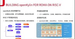
The world's first RISC-V development laptop ROMA was officially released, and it is equipped with openKylin (Open Kylin) domestic operating system by default. The official did not announce the specific parameters of ROMA at this meeting. The PPT only disclosed the use of 4-core 12/22nm processors and 4/8/16GB memory.


- Status
- Not open for further replies.
