Chinese semiconductor industry

Status
Not open for further replies.

tphuang

Lieutenant General
Staff member
Super Moderator
VIP Professional
Registered Member
Please, Log in or Register to view URLs content!
东阳华芯:开启新征程

去年,华懋科技、徐州博康在浙江省东阳市联合设立合资企业——东阳华芯电子材料有限公司,着力于实现我国高端干湿法ArF和KrF光刻胶产品及相关光刻材料工艺与性能的全面提升。对此,徐州博康向爱集微阐述,公司对东阳华芯的前景高度看好并寄予厚望。

公司指出,东阳华芯预计2023年中投入使用,为正在加速的半导体光刻胶国产化提供更多的中高端光刻材料的开发及产能支撑。东阳华芯着力于实现我国高端干湿法ArF\KrF光刻胶产品及相关光刻材料工艺与性能的全面提升,通过稳定持续的量产供应,提高半导体光刻胶的国产化水平。新的生产基地“拟建设年产8000吨中高端半导体光刻材料”,产品为中高端半导体光刻胶及其配套材料,主要包括ArF光刻胶系列、KrF光刻胶系列、半导体厚膜封装胶,半导体用光敏性聚酰亚胺(PSPI)等。

写在最后

徐州博康去年投产了年产1100吨光刻材料及1万吨电子溶剂新工厂,经过多方审核评估,于2021年底正式生产,是国内最大的半导体光刻材料生产基地,包含电子级溶剂,光刻胶单体,树脂及光刻胶的一体化生产体系。目前已通过多家FAB客户验厂审核并获得合格供应商资质。博康工厂光刻胶车间的设计产能为2500加仑/月,正在稳步提升产能利用率。

秉承创新、诚信、精进的企业宗旨,光刻胶单体产品目前已经打入了国内外光刻胶公司的供应体系,已经成为JSR、东进、TOK、陶氏、住友、锦湖等国际大厂的光刻材料稳定供应商,同时很好的解决了国内单体产品的技术痛点,并打破了日本美国对单体产品的垄断地位,已经实现了完全国产化,占全球市场份额的18%,已覆盖全球80%的光刻胶单体产品技术。徐州博康的研发导入进程进入提速期,实现了由质及量的“聚合效应”,随着市场占有率的不断提高,企业的增长曲线也在朝向立体化方向发展。
Looks like Xuzhou B&C Chemicals does have quite the production. A huge supplier of Photoresist monomers to Japanese companies and they are increasing their own production with this new 8000t medium/high end photoresist material factory that will go live this year.

They also had 1100t photoresist material plant that went into product in 2021. Looks like it has 18% global market share in monomer and covers 80% of photoresist monomer products.

Please, Log in or Register to view URLs content!
晶瑞电材此前曾表示,子公司瑞红(苏州)电子化学品股份有限公司2018年完成了国家重大科技项目02专项“i线光刻胶产品开发及产业化”项目后,i线光刻胶产品向中芯国际、合肥长鑫、华虹半导体、晶合集成等国内知名半导体企业批量供货。高端KrF光刻胶分辨率达到0.25-0.13μm,通过部分重要客户测试,计划2022年底批量供应;ArF光刻胶研发工作正有序开展。眉山晶瑞年产1200吨光刻胶项目计划2022年底建成。

徐州博康成立于2007年,深耕光刻材料领域十余年,实现了从单体、光刻胶专用树脂、光酸剂及终产品光刻胶的国产化自主可控的供应链,在KrF、ArF光刻胶的验证、导入、量产进展效率瞩目,为国内半导体光刻胶领域少有的垂直一体化企业。2021年华懋科技通过产业基金的形式布局光刻材料业务板块,子公司东阳凯阳持有徐州博康约26%股份,是徐州博康第二大股东。
Another play Jingrui chemical started KRF production by end of 2022 (supposedly)

Xuzhou B&C is different in that it controls the entire supply chain including monomers, photoresist-specific resins, photoacids and the end product photoresist. It has been validating and producing KRF, ARF photoresists.
 

tphuang

Lieutenant General
Staff member
Super Moderator
VIP Professional
Registered Member
Please, Log in or Register to view URLs content!
在国产光刻胶这条赛道上,徐州博康已实现“单体——树脂、光酸——光刻胶”产业链全覆盖。在过去的十余年中,徐州博康完成中高端半导体光刻胶材料产品的国际化销售,逐步建立起了全面自主可控的光刻胶供应链。

据悉,单体作为光刻胶曝光显影功能的原始载体,直接决定着光刻胶的性能,成本占比高达60-80%。傅志伟介绍,徐州博康前身上海博康从2005年开始研发单体,并掌握单体提纯的先进工艺,能够把单体的金属离子杂质含量控制在1ppb以下。
Emphasized here that Xuzhou B&C produces monomer, resin, photo acid & photoresist. It built the entire photoresist supply chain and has been exporting medium to high end photoresist material Monomer accounts for 60 to 80% of photoresist cost.
 

european_guy

Junior Member
Registered Member
They also had 1100t photoresist material plant that went into product in 2021. Looks like it has 18% global market share in monomer and covers 80% of photoresist monomer products.

Sorry to be pedantic, but maybe they refer to lithography material in general. Regarding specifically photoresist they wrote

博康工厂光刻胶车间的设计产能为2500加仑/月
The design capacity of the photoresist workshop of Bokang factory is 2500 gallons per month -> 10t/month -> around 100t/year

Very impressive that they are already fully independent on photoresist monomers. This is an unexpected good news, it means US cannot easily cripple photoresist manufacturers, because the raw material is already produced in China.


Another play Jingrui chemical started KRF production by end of 2022 (supposedly)

The threat, real or not, of banning photoresist from Japan (that already did this trick to Korea) will unleash a race among Chinese Chemical firms to reach production volumes as soon as possible, now that the doors of the fabs will fully open....the standard multi-year validation time is going to shrink a lot! :)

I understand that fabs care about yields...but they care even more to keep the production running, and if the yields are not good, it is up to the govt. to foot the bill in this very special times. For instance, last week's multi-bilion investment in YMTC can be an example of govt. support. IMHO I'd speculate that it can be a defensive investment, more than for supporting an aggressive capacity expansion. The investment may be used to "cushion" the extra costs for the ultra-accelerated localization efforts that YMTC is going to face.
 

tokenanalyst

Brigadier
Registered Member

The gallium oxide vertical trench gate field effect transistor was developed for the first time! The research group of Professor Long Shibing from the University of Science and Technology of China has made important progress in the field of gallium oxide power electronic devices in cooperation with the processing platform of Suzhou Institute of Nanotechnology, Chinese Academy of Sciences​


Recently, the research group of Professor Long Shibing, School of Microelectronics, University of Science and Technology of China, and the processing platform of Suzhou Institute of Nanotechnology, Chinese Academy of Sciences have made important progress in the field of gallium oxide power electronic devices . Using oxygen atmosphere annealing and N ion implantation technologies, gallium oxide has been developed for the first time. Vertical Trench Gate Field Effect Transistor .

Power semiconductor devices are the core components in power electronic systems, mainly used for power conversion of power equipment and high power in control circuits. Application scenarios include industrial control, renewable energy and new energy systems, electric vehicles, rail transit, etc.

With the development of new energy vehicles and other industries and their ever-increasing requirements for power system control capabilities, and traditional semiconductor materials such as Si are gradually approaching the physical limit, gallium oxide, as a new generation of power semiconductor materials, has a large bandgap, shock The high cross-field strength is expected to play an important role in the field of power devices in the future.

In addition, gallium oxide semiconductor materials can be grown by the melt method, and will have more advantages in cost than materials such as SiC and GaN in the future.

At present, gallium oxide materials are facing an important difficulty : it is difficult to achieve p-type doping of gallium oxide , which leads to problems such as difficulty in realizing enhancement mode and improving power quality factor in gallium oxide field effect transistors. Gallium oxide vertical field effect transistors are suitable for the preparation of high-voltage and high-current devices. Compared with the preparation of horizontal structure MBE samples, the material has a lower cost.

Among the several structures of gallium oxide vertical transistors, although FinFET has excellent performance, the process is difficult and it is difficult to achieve mass production. Therefore, there is an urgent need to design a new vertical gallium oxide transistor , overcome the current blocking layer technology required by the enhancement transistor, and use the current blocking layer to prepare a newly designed gallium oxide vertical gate transistor.

research work


In the work reported in this report, the current blocking layer of the device was prepared by oxygen atmosphere annealing and nitrogen (N) ion implantation processes , and gallium oxide that does not require P-type doping technology was developed in conjunction with the gate groove etching process. Vertical trench field effect transistor structure.

MBXY-CR-97fed4e17496e0ec0d4371949199e8bf.png

Figure 1 (a) Schematic diagram of the structure of GaO vertical trench gate field effect transistor; (b) Schematic diagram of the working principle of the device; (c) The output curve of N ion implanted transistor; (d) The performance of the reported GaO vertical field effect transistor Compare.

The current blocking layer formed by oxygen atmosphere annealing and N ion implantation can effectively isolate the current path between the source and drain of the transistor. When a positive gate voltage is applied, a conductive channel for electron accumulation will be formed on the side wall of the gate groove, realizing the Current regulation.

Annealing gallium oxide in an oxygen atmosphere can form compensation defects on the surface, thereby forming a high resistance layer. Oxygen atmosphere annealing process is a relatively unique technical means of gallium oxide. This method is inspired by one of the secrets of the success of silicon technology - the oxygen atmosphere annealing of semiconductor silicon. Similar to silicon annealing in an oxygen atmosphere can form a high-resistance surface layer, gallium oxide uses this method to prepare a current blocking layer (compared to ion implantation), which has the characteristics of fewer defects, no diffusion, and low cost.

N ion implantation MOSFET is based on industrial high-energy ion implantation equipment, adopts N ion implantation doping process, when the N implantation concentration is 5×10^18cm-3, the threshold voltage of the prepared vertical groove gate MOSFET reaches 4.2V (@1A/cm2) , the saturation current density is as high as 702.3A/cm2, and the on-resistance is 10.4mΩ·cm2 . In addition, by adjusting the concentration of N ion implantation, the breakdown voltage of the device can reach 534V, which is the highest value of current blocking layer gallium oxide MOSFET devices, and the power quality factor exceeds the theoretical limit of silicon unipolar devices. The two works have found new technical routes and structural solutions for gallium oxide transistors.

Please, Log in or Register to view URLs content!
 

theorlonator

Junior Member
Registered Member
China AI groups targeted by US sanctions have found ways to obtain restricted technology by using cloud providers and rental arrangements with third parties, as well as purchasing the chips through subsidiary companies. Rental system is a good, albeit more expensive, alternative.
"Privately controlled cloud computing companies also provide access to high-end US chips. AI-Galaxy, a Shanghai-based cloud computing company founded by former employees from Nvidia and AliCloud, charges $10 for one-hour access to eight of its A100 Nvidia chips. The ability of Chinese AI groups to continue accessing Nvidia’s crucial high-end chips and other cutting-edge technology underlines the challenge the US faces in enforcing its trade restrictions against Chinese companies."

Made me LOL really hard.
 

tokenanalyst

Brigadier
Registered Member
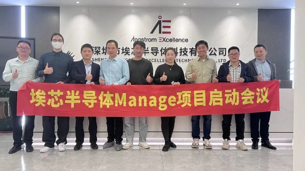
Aixin Semiconductor has reached a cooperation with Xinchen Technology and officially launched the "PDM project"


Recently, AE Semiconductor has reached a cooperation with Xinchen Technology to officially launch the "PDM project" to improve the product R&D management process and build a unified data management platform for the sector, so as to improve efficiency and reduce costs, further realize the digital transformation of enterprises, and enhance the core competitiveness of enterprises force.
More than a dozen representatives from both sides, including the R&D manager of AE semiconductor, the production manager of AE semiconductor, the technical director of Xinchen Technology, and the project leader, attended the meeting. This meeting mainly discussed and exchanged around the project implementation scope of Aixin Semiconductor.
7711258e4eb44f519dfabff5b9b79079.jpg


Aixin Semiconductor

Established in October 2020, Shenzhen Aixin Semiconductor Technology Co., Ltd. specializes in the R&D, manufacturing and sales of semiconductor front-end measurement and testing equipment. The company's products cover optical thin film measurement, optical critical dimension measurement, X-ray thin film measurement, X-ray material property measurement, X-ray composition and surface pollution measurement and other series of products and solutions. The product specifications match the international advanced level. The company has more than 1,000 square meters of R&D and production plants in Shenzhen, including a thousand-level assembly and commissioning clean room, a hundred-level and ten-level laboratory clean room.
The company's core R&D team is strong, composed of top technical experts in the global semiconductor industry and senior researchers from global scientific research institutions. The company has formed an international scientific research team with global comprehensive R&D capabilities in the field of semiconductor equipment. While focusing on independent research and development of core technologies, the company actively deploys global technical cooperation and market development, and has achieved technological breakthroughs in multiple measurement fields.

Xinchen Information Technology (Shenzhen) Co., Ltd.
Xinchen Information Technology (Shenzhen) Co., Ltd. is a value-added reseller of SOLIDWORKS in South China. The company was established in 2015. It is a service team specializing in the sales, technical support and training of computer professional design software, providing complete solutions for the manufacturing industry in product development. CAD/CAM/CAE/PDM/EDA series integrated solutions.
According to the needs of customers in different industries, we provide customized product solutions, and help customers succeed through professional teams and efficient and scientific implementation. At present, branch offices are set up in Shenzhen, Dongguan and other regions to provide localized services for more customers. According to customer needs, provide customized product solutions, and help customers achieve success through professional teams, scientific and efficient implementation.
 

bzhong05

New Member
Registered Member
This is from havok? We can assume it's legit then?
From this post -
Please, Log in or Register to view URLs content!


由于国内现在只做不说,低调,所以很多公开的咨询公司的调查报告基本全部失真,比如说国内光刻胶厂商市占率只有1%,其余全部是外资,这是不对的。同理还有长江存储市占率只有6%,上海微电子前道GKJ市占率为0,这些都不准确。以上微为例,它的90nm GKJ已经量产且批量供货,干式arf duv gkj也量产且批量供货,由于这些机型的热销甚至导致原产线饱和,上微甚至要在今年扩产新增年产20台arfi duv gkj产线专供arfi gkj。目前所有接受上微前道gkj的单位都不得公开宣传,导致很多带节奏的文章仍然认为有且仅有1台90样机放在角落里吃灰。

Apparently, the original poster said that many industry reports do not reflect reality such as the market share of domestic photoresist companies constituting just 1%, YMTC has 6% market share or SMEE having 0% marketshare. They also claimed that SMEE has realized full production capacity and would even increase production this year to 20 ArFI DUV machines. All companies receiving SMEE machines are prohibited from publicizing the info so people still assume there is only one obsolete 90nm machine.

How legit is this info based on what havok had previously said?
 
Status
Not open for further replies.
Top