You are using an out of date browser. It may not display this or other websites correctly.
You should upgrade or use an alternative browser.
You should upgrade or use an alternative browser.
Chinese semiconductor industry
- Thread starter Hendrik_2000
- Start date
- Status
- Not open for further replies.
New progress in the construction of major platforms in Shenzhen! Inauguration of Electronic Components and Integrated Circuits International Trade Center
The construction of the trading center plays an active role in assisting the digital transformation of enterprises, promoting the high-quality development of enterprises, serving high-end, high-quality and high-tech modern industrial systems, etc., and promoting the reduction of costs and increasing efficiency of the industrial chain and supply chain, and striving to improve the resilience of the industrial chain and supply chain The level of safety and security is a milestone, and it is expected to accelerate the transformation of the resource endowment advantages of the domestic ultra-large-scale market to the competitive advantages of the global market, and provide important support for a new round of technological revolution.
SMIC Thermal Technology completed the Pre-A round of financing of tens of millions of yuan, focusing on the field of infrared quantum material imaging chips.
SMIC Thermal Technology (Beijing) Co., Ltd. (hereinafter referred to as "SMIC") completed the Pre-A round of financing of tens of millions of yuan, led by Shenzhen Yiyuan Aerospace Private Equity Fund Management Co., Ltd. led the investment, followed by Founder Hesheng and Taiyou Fund.
It is reported that this round of financing will be used for the construction of 8-inch wafer-level chip and module production lines for colloidal quantum dot infrared detectors and the application research and development of products, which can be applied in the fields of industry, aerospace, automobiles, and consumer electronics. Imaging chips provide new technical architectures and solutions in many fields.
SMIC Thermal Technology is a high-tech enterprise focusing on the field of infrared quantum material imaging chips . It can realize the preparation of short, medium and long-wave focal plane detectors with different array sizes of 320×256, 640×512 and 1280×1024. The comprehensive indicators It is domestically advanced; it is the first to create a vertically stacked different-bandgap quantum dot process, which provides a new solution for the realization of short/short, short/medium, medium/long and other two-color detection.
The company's R&D center covers an area of about 1,300 square meters, with functions including chip substrate preparation, material synthesis, chip production, chip testing, machine assembly, environmental testing and system testing, among which the ultra-clean production workshop covers an area of 500 square meters. Equipped with two purification levels of class 100 and class 1000, it has professional production equipment and process realization conditions for the design, manufacture, testing, and packaging of micro-nano semiconductor optoelectronic devices, and can independently complete the preparation, packaging and testing of short-wave and mid-wave infrared imaging chips.
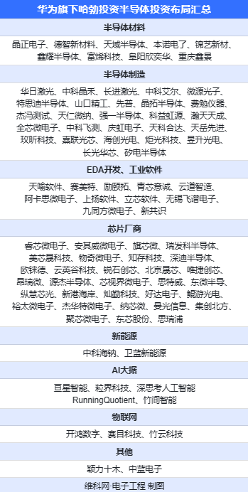
it is a list of Huawei hubble to invest in the domestic semiconductor industry... the semiconductor material should add Bokang
The introduction of BIWIN's self-developed test system + Advantest high-end equipment further consolidated its advanced packaging and testing capabilities
the Advantest T5503HS2 mass production test system was successfully installed in Biwin's advanced manufacturing plant, further strengthening the company's own full-stack memory chip testing capabilities. T5503HS2 has a test rate of up to 8Gbps and a test accuracy of ±45 picoseconds , which meets the high-frequency and high-speed test requirements of BIWIN’s DDR5 and LPDDR5 products, and can also test DDR4, LPDDR4/4X and high-bandwidth memory devices.
the Advantest T5503HS2 mass production test system was successfully installed in Biwin's advanced manufacturing plant, further strengthening the company's own full-stack memory chip testing capabilities. T5503HS2 has a test rate of up to 8Gbps and a test accuracy of ±45 picoseconds , which meets the high-frequency and high-speed test requirements of BIWIN’s DDR5 and LPDDR5 products, and can also test DDR4, LPDDR4/4X and high-bandwidth memory devices.
Guangli Technology: Localized packaging and testing equipment is already in the mass production and sales stage
Jiwei.com News On February 8, Guangli Technology stated on the investor interaction platform that the company's localized packaging and testing equipment is currently in the mass production and sales stage, and the performance of the products in all aspects has been highly recognized by customers.
According to him, the company has independent technology and production capacity in the cutting process of the packaging and testing industry, such as semiconductor precision cutting equipment, core components, and key consumables, and has a complete product layout in semiconductor cutting and scribing equipment. China has a relatively high proportion of the packaging and testing industry. The company benefits from localization substitution, the development of the semiconductor industry and the current market competition pattern. The company's products have a large space for substitution.
As for the production of the plant, Guangli Technology said that the installation and commissioning of the newly purchased equipment in the new plant of the company's airport have basically been completed, and it is expected to be put into production by the end of the first quarter. At present, the original factory area can meet the delivery of existing orders. The production capacity of the original factory will be gradually transferred to the new factory. "The company will rationally adjust the production capacity of new and old factories based on factors such as sales forecast and production scheduling in the next stage. Through the above adjustments, it will better meet the delivery needs of current and future orders."
work has now started on this factory in Beijing.
BOE tech is putting in 29 billion RMB investment into a new plant producing 6th gen Semiconductor display.
Product includes VR display, miniLED and other displays.
designed capacity is 50k wpm. Looking to start mass production in 2025. And reach mass production in 2026.
- Status
- Not open for further replies.


