Chinese semiconductor industry

Status
Not open for further replies.

tokenanalyst

Brigadier
Registered Member

State-level specialization and special new "little giant", the head supplier of core ceramic components for semiconductor equipment, Kema Technology will be held on the GEM for the first time on January 20​


China Securities Network News (Wang Luo) On the evening of January 13, the Shenzhen Stock Exchange announced that Suzhou Kema Material Technology Co., Ltd. (referred to as: Kema Technology) will be listed on the GEM on January 20.
Kema Technology is the leading enterprise of advanced ceramic materials and components in the domestic semiconductor field, and one of the leading enterprises in the surface treatment of the domestic display panel field. According to the data, Kema Technology officially applied for the Shenzhen Stock Exchange's GEM IPO on June 29, 2022 and was accepted. The listing plans to issue no more than 120.33 million shares to the public. The raised funds will be used for the "advanced material production base project" and "pan-semiconductor Core parts processing and manufacturing projects", "R&D center construction projects" and supplementary working capital.

Since its establishment in April 2009, Kema Technology has been focusing on the R&D, manufacturing, sales, service of advanced ceramic material parts and surface treatment services for pan-semiconductor equipment. The main products include advanced ceramic material parts, etc., and provide customers with precision Surface treatment services such as cleaning, anodizing and spraying; in addition to the semiconductor field, the company's advanced ceramic materials and products are also widely used in display panels, LEDs, photovoltaics and other pan-semiconductor fields, as well as electronic (including lithium battery) material powders Equipment and production processes in the fields of crushing and grading, fuel cell manufacturing, chemical environmental protection, automobile manufacturing, biomedicine, and traditional textile and paper making.
Break the international monopoly and fill the blank of domestic enterprises in the field of advanced ceramics

Among them, as a representative enterprise in the field of advanced ceramics in China and one of the few domestic enterprises that have mastered the core technology of advanced ceramics for semiconductor equipment, from material formulation to parts manufacturing, and achieved overseas scale sales, Kema Technology has formed a network of products through independent research and development. The core technology system composed of material formula and production process has filled the blank of Chinese enterprises in the advanced ceramic industry, and many key technical indicators of advanced ceramic material parts have reached domestic leading and international mainstream levels. According to public materials, some models of the company's ceramic heater products have passed customer verification and entered small-batch production.

Please, Log in or Register to view URLs content!
 

tokenanalyst

Brigadier
Registered Member

North Huachuang's net profit is expected to exceed 2.1 billion, an increase of 8 times in four years.​


On the evening of January 11, North Huachuang released the 2022 annual performance forecast. The company expects to achieve annual operating income of 13.5 billion to 15.6 billion yuan, a year-on-year increase of more than 3.8 billion yuan; the estimated profit is 2.1 billion to 2.6 billion yuan, a year-on-year increase of more than 1 billion yuan, double that of the same period last year.
A reporter from Changjiang Commercial Daily found that starting in 2018, NAURA’s main business profitability continued to release. The lower limit of the expected profit in 2022 is about 8 times higher than that in 2018.
North Huachuang is mainly engaged in the R&D, production, sales and technical services of basic semiconductor products, and is a mainstream high-end electronic technology equipment supplier in China. In recent years, the company has stepped up the implementation of industrial layout, and its operating performance and asset scale have grown rapidly. At the end of the third quarter of 2022, the company's total assets were 40.896 billion yuan, an increase of more than 30 billion yuan from 10.001 billion yuan in 2018.
Making efforts in the high-end market is an important factor for the rapid growth of NAURA's operating performance. In 2019 and 2021, the company raised a total of 10.5 billion yuan in two fixed increase. These funds are mainly used for high-end production capacity layout, project research and development, etc.
The annual pre-profit exceeds 2.1 billion to a new high
The operation of North Huachuang achieved another bumper harvest.
The company expects to realize a net profit of 1.9 billion yuan to 2.4 billion yuan after deducting non-recurring gains and losses, which will increase by 1.093 billion yuan to 1.593 billion yuan compared with 807 million yuan in the same period last year, with a year-on-year growth rate of 135.52%-197.50%. .
The annual profit is at least 2.1 billion yuan, which is unprecedented for NAURA and has reached a record high.
Such high-speed growth in operating performance has laid a solid foundation in the first three quarters of last year. According to the third quarterly report of last year, in the first nine months, the company realized operating income of 10.012 billion yuan, a year-on-year increase of 62.19%.
From a single quarter perspective, in the first, second, and third quarters of last year, the company realized net profits of 206 million yuan, 548 million yuan, and 931 million yuan, respectively, a year-on-year increase of 183.18%, 130.87%, and 167.71%, respectively. 100 million yuan, 490 million yuan, and 831 million yuan, a year-on-year increase of 382.23%, 154.18%, and 176.76%. In the fourth quarter, the company expects net profit and non-net profit to be 414 million yuan to 914 million yuan, and 424 million yuan to 924 million yuan respectively. If the median is taken, both net profit and non-net profit after deduction have increased significantly compared with the same period of the previous year.
The predecessor of North Huachuang was Seven Star Electronics, which was listed on the Shenzhen Stock Exchange in March 2010. In 2016, Sevenstar Electronics and North Microelectronics implemented a joint reorganization to form North Huachuang, which included North Microelectronics, a leading enterprise in the domestic semiconductor equipment industry, under its umbrella, and jointly built a flagship platform for China's high-end integrated circuit equipment industry.
After the joint reorganization, the new North Huachuang came out, and its operating performance continued to improve. From 2016 to 2021, the company's net profits were 93 million yuan, 126 million yuan, 234 million yuan, 309 million yuan, 537 million yuan, and 1.077 billion yuan, a year-on-year increase of 46.51%, 35.21%, 86.05%, and 32.24%. , 73.75%, 100.66%. During the same period, the company's operating income increased from 1.622 billion yuan to 9.683 billion yuan. Like net profit, it has also grown rapidly for 6 consecutive years.
4 years to invest 8 billion in research and development
NAURA's operating performance has doubled for two consecutive years, which is related to the company's focus on the high-end market and the rising market prosperity.
In recent years, North Huachuang has made full use of the capital market for financing and invested heavily in construction.
The 2022 semi-annual report disclosed that in the 2019 fundraising project "High-end Integrated Circuit Equipment R&D and Industrialization Project", the engineering construction project was completed last year and will be fully put into operation in the first half of 2022, and the R&D and industrialization verification projects are continuing to advance . The "High-precision Electronic Components Industrialization Base Expansion Project" has been completed as planned and has reached the planned production capacity. In the first half of last year, its economic benefit was 35.4744 million yuan, which reached the expected benefit.
In November 2021, North Huachuang once again implemented fixed increase fundraising and successfully raised 8.5 billion yuan. The funds raised this time will be used for the construction of the expansion project of the semiconductor equipment industrialization base (Phase IV), the high-end semiconductor equipment research and development project, and the expansion project of the high-precision electronic component industrialization base (Phase III) and other construction and supplementary working capital.
According to the special report on the deposit and actual use of raised funds for the half year of 2022 disclosed by NAURA, the 1.824 billion yuan fundraising supplementary working capital has been completed, and the three physical projects have all started construction. As of the end of June 2022, the investment progress of the three physical projects is 7.61%, 46.32%, and 24.20%, respectively.
The two fixed increase funds raised a total of 10.5 billion yuan, and these funds were mainly used for high-end production capacity expansion and project research and development. It can be seen that the company is making every effort to advance into the high-end field.​

Please, Log in or Register to view URLs content!
 

tonyget

Senior Member
Registered Member
Please, Log in or Register to view URLs content!

Comparison: Latest 3D NAND Products from YMTC, Samsung, SK hynix and Micron​

With their 232-layer Xtacking 3.0 readily available in commercial products, YMTC appears to have pulled ahead of the pack for the moment. TechInsights ran a comparison of the YMTC 232-L against 128- and 176- layer solutions from Samsung, SK hynix, and Micron, looking at factors like die size, bit density, active layers, word line pitch, and more.

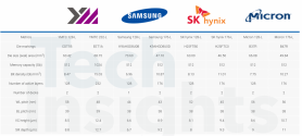
As TechInsights continues analysis of YMTC 232-Layer 3D NAND, we thought a comparison was in order. We compared the YMTC’s 1024 Gb (1 Tb) triple level cell (TLC) 232-L 3D NAND with recent 512 Gb TLC 3D NAND dies (see Table 1) we examined from Samsung, SK hynix and Micron.

001.png

Up to and including 128-L, 3D NAND had been dominated by Samsung with its single deck process, enabled by its ultra-high aspect ratio (UHAR) hole etch. Samsung still leads the pack with the smallest word line (WL) pitch, which allows more layers to be stacked while minimizing the impact to the process requirements for vertical channel (VC) height and slit depth. While it appears that Samsung may have had the lowest process cost for 128-L, it did not have the lowest die size. This is significant, because the lower the die size area, the more dies that can be fabricated on a 300 mm wafer, and thus more profit.

Samsung started to adopt the cell over periphery (COP) approach at 176-L (Samsung’s 7th-generation 3D NAND) which lead to a significant die size reduction from its 128-L to 176-L. Similar approaches had been used by Micron from 32-L (Micron’s 1st-generation 3D NAND) onwards, which Micron termed as CMOS under array, CuA, and by SK hynix from 96-L (SK hynix’s 4th-generation 3D NAND) onwards, which SK hynix termed as 4D NAND, periphery under cell or PUC). YMTC applied Xtacking at 64-L (YMTC’s 2nd-generation 3D NAND) to achieve similar benefit of reduced die size, by having the memory array over the periphery circuits. The reduced die size along with increased active word lines (AWLs) drives up the bit density.

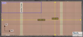
The recently acquired YMTC 232-L six-plane 1 Tb TLC die with center X-decoder (see Figure 1) has the highest bit density of 15.03 Gb/mm2.

002.jpg
Figure 1: Die image of YMTC 232-L 1 Tb die. TechInsights, 2022.


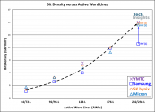
Chart 1 shows bit density (Gb/mm2) versus number of AWLs. We expect the bit density of the upcoming 232/238L dies to reach approximately 15 Gb/mm2. At ISSCC 2022, Samsung 2xx-L test vehicle (with four-plane 1 Tb TLC die with edge X-decoder) has a bit density of 11.55 Gb/mm2 [1]. We expect the bit density to increase to above 14.5 Gb/mm2 when the production mask set is used. SK hynix 238-L six-plane 1 Tb TLC die with center X-decoder is estimated to be 14.75 Gb/mm2 [2] with 34 % increased from previous generation. Micron 232-L six-plane 1 Tb TLC die is stated to be 14.60 Gb/mm2 [3].

003.png
Chart 1: Bit Density versus Active Word Lines (AWLs). TechInsights, 2022.

Several TechInsights Memory Floorplan and Advanced Memory Essentials reports informed this comparison article. Subscribers to our NAND & DRAM channels can access the reports below in our Platform. If you are not a subscriber, but are interested in our reports, please
Please, Log in or Register to view URLs content!
.


004.png
Table 2: Information sources for Chart 1. TechInsights, 2022.

At 232/238-L, YMTC showed the highest bit density and Samsung is projected to have the lowest bit density. What does this mean for the NAND market? Does this mean that Samsung will be dropping out of the race? Certainly not. One of the more important factors to consider is the overall cost, and thus the metric of cost/bit is the most ideal data for comparison. TechInsights, through our recent acquisition of IC Knowledge, is working toward calculating cost/bit, and should have this information available in 2023. IC Knowledge is the world leader in cost modeling of semiconductors. Click
Please, Log in or Register to view URLs content!
if you would like to learn more about this acquisition.

Reference:​

[1] M. Kim et al., "A 1Tb 3b/Cell 8th-Generation 3D-NAND Flash Memory with 164MB/s Write Throughput and a 2.4Gb/s Interface," 2022 IEEE International Solid- State Circuits Conference (ISSCC), 2022, pp. 136-137, doi: 10.1109/ISSCC42614.2022.9731640.
[2] SK hynix Press Release:
Please, Log in or Register to view URLs content!

[3] Micron Product Information:
Please, Log in or Register to view URLs content!

[4] TechInsights Press Release:
Please, Log in or Register to view URLs content!

More of our coverage on YMTC’s Xtacking 3.0
Please, Log in or Register to view URLs content!
 

siegecrossbow

General
Staff member
Super Moderator
Please, Log in or Register to view URLs content!

Comparison: Latest 3D NAND Products from YMTC, Samsung, SK hynix and Micron​

With their 232-layer Xtacking 3.0 readily available in commercial products, YMTC appears to have pulled ahead of the pack for the moment. TechInsights ran a comparison of the YMTC 232-L against 128- and 176- layer solutions from Samsung, SK hynix, and Micron, looking at factors like die size, bit density, active layers, word line pitch, and more.

As TechInsights continues analysis of YMTC 232-Layer 3D NAND, we thought a comparison was in order. We compared the YMTC’s 1024 Gb (1 Tb) triple level cell (TLC) 232-L 3D NAND with recent 512 Gb TLC 3D NAND dies (see Table 1) we examined from Samsung, SK hynix and Micron.

View attachment 105316

Up to and including 128-L, 3D NAND had been dominated by Samsung with its single deck process, enabled by its ultra-high aspect ratio (UHAR) hole etch. Samsung still leads the pack with the smallest word line (WL) pitch, which allows more layers to be stacked while minimizing the impact to the process requirements for vertical channel (VC) height and slit depth. While it appears that Samsung may have had the lowest process cost for 128-L, it did not have the lowest die size. This is significant, because the lower the die size area, the more dies that can be fabricated on a 300 mm wafer, and thus more profit.

Samsung started to adopt the cell over periphery (COP) approach at 176-L (Samsung’s 7th-generation 3D NAND) which lead to a significant die size reduction from its 128-L to 176-L. Similar approaches had been used by Micron from 32-L (Micron’s 1st-generation 3D NAND) onwards, which Micron termed as CMOS under array, CuA, and by SK hynix from 96-L (SK hynix’s 4th-generation 3D NAND) onwards, which SK hynix termed as 4D NAND, periphery under cell or PUC). YMTC applied Xtacking at 64-L (YMTC’s 2nd-generation 3D NAND) to achieve similar benefit of reduced die size, by having the memory array over the periphery circuits. The reduced die size along with increased active word lines (AWLs) drives up the bit density.

The recently acquired YMTC 232-L six-plane 1 Tb TLC die with center X-decoder (see Figure 1) has the highest bit density of 15.03 Gb/mm2.

View attachment 105313
Figure 1: Die image of YMTC 232-L 1 Tb die. TechInsights, 2022.


Chart 1 shows bit density (Gb/mm2) versus number of AWLs. We expect the bit density of the upcoming 232/238L dies to reach approximately 15 Gb/mm2. At ISSCC 2022, Samsung 2xx-L test vehicle (with four-plane 1 Tb TLC die with edge X-decoder) has a bit density of 11.55 Gb/mm2 [1]. We expect the bit density to increase to above 14.5 Gb/mm2 when the production mask set is used. SK hynix 238-L six-plane 1 Tb TLC die with center X-decoder is estimated to be 14.75 Gb/mm2 [2] with 34 % increased from previous generation. Micron 232-L six-plane 1 Tb TLC die is stated to be 14.60 Gb/mm2 [3].

View attachment 105314
Chart 1: Bit Density versus Active Word Lines (AWLs). TechInsights, 2022.

Several TechInsights Memory Floorplan and Advanced Memory Essentials reports informed this comparison article. Subscribers to our NAND & DRAM channels can access the reports below in our Platform. If you are not a subscriber, but are interested in our reports, please
Please, Log in or Register to view URLs content!
.


View attachment 105315
Table 2: Information sources for Chart 1. TechInsights, 2022.

At 232/238-L, YMTC showed the highest bit density and Samsung is projected to have the lowest bit density. What does this mean for the NAND market? Does this mean that Samsung will be dropping out of the race? Certainly not. One of the more important factors to consider is the overall cost, and thus the metric of cost/bit is the most ideal data for comparison. TechInsights, through our recent acquisition of IC Knowledge, is working toward calculating cost/bit, and should have this information available in 2023. IC Knowledge is the world leader in cost modeling of semiconductors. Click
Please, Log in or Register to view URLs content!
if you would like to learn more about this acquisition.

Reference:​

[1] M. Kim et al., "A 1Tb 3b/Cell 8th-Generation 3D-NAND Flash Memory with 164MB/s Write Throughput and a 2.4Gb/s Interface," 2022 IEEE International Solid- State Circuits Conference (ISSCC), 2022, pp. 136-137, doi: 10.1109/ISSCC42614.2022.9731640.
[2] SK hynix Press Release:
Please, Log in or Register to view URLs content!

[3] Micron Product Information:
Please, Log in or Register to view URLs content!

[4] TechInsights Press Release:
Please, Log in or Register to view URLs content!

More of our coverage on YMTC’s Xtacking 3.0
Please, Log in or Register to view URLs content!

YMTC is pretty much Carl. Cucked hard but back on his feet and denying the abuser satisfaction.
 

bzhong05

New Member
Registered Member
Another piece of news regarding chip sanctions:

Please, Log in or Register to view URLs content!

AMSTERDAM, Jan 16 (Reuters) - The top Dutch trade official said the Netherlands will not summarily accept new U.S. restrictions on exporting chip-making technology to China, and is consulting with European and Asian allies.

Trade Minister Liesje Schreinemacher spoke on Sunday on the television show Buitenhof ahead of a visit to the U.S. by Dutch Prime Minister Mark Rutte on Tuesday, when he is expected to discuss export policy with President Joe Biden.
 

SanWenYu

Captain
Registered Member

State-level specialization and special new "little giant", the head supplier of core ceramic components for semiconductor equipment, Kema Technology will be held on the GEM for the first time on January 20​


China Securities Network News (Wang Luo) On the evening of January 13, the Shenzhen Stock Exchange announced that Suzhou Kema Material Technology Co., Ltd. (referred to as: Kema Technology) will be listed on the GEM on January 20.
Kema Technology is the leading enterprise of advanced ceramic materials and components in the domestic semiconductor field, and one of the leading enterprises in the surface treatment of the domestic display panel field. According to the data, Kema Technology officially applied for the Shenzhen Stock Exchange's GEM IPO on June 29, 2022 and was accepted. The listing plans to issue no more than 120.33 million shares to the public. The raised funds will be used for the "advanced material production base project" and "pan-semiconductor Core parts processing and manufacturing projects", "R&D center construction projects" and supplementary working capital.

Since its establishment in April 2009, Kema Technology has been focusing on the R&D, manufacturing, sales, service of advanced ceramic material parts and surface treatment services for pan-semiconductor equipment. The main products include advanced ceramic material parts, etc., and provide customers with precision Surface treatment services such as cleaning, anodizing and spraying; in addition to the semiconductor field, the company's advanced ceramic materials and products are also widely used in display panels, LEDs, photovoltaics and other pan-semiconductor fields, as well as electronic (including lithium battery) material powders Equipment and production processes in the fields of crushing and grading, fuel cell manufacturing, chemical environmental protection, automobile manufacturing, biomedicine, and traditional textile and paper making.
Break the international monopoly and fill the blank of domestic enterprises in the field of advanced ceramics

Among them, as a representative enterprise in the field of advanced ceramics in China and one of the few domestic enterprises that have mastered the core technology of advanced ceramics for semiconductor equipment, from material formulation to parts manufacturing, and achieved overseas scale sales, Kema Technology has formed a network of products through independent research and development. The core technology system composed of material formula and production process has filled the blank of Chinese enterprises in the advanced ceramic industry, and many key technical indicators of advanced ceramic material parts have reached domestic leading and international mainstream levels. According to public materials, some models of the company's ceramic heater products have passed customer verification and entered small-batch production.
Please, Log in or Register to view URLs content!

According to Guancha, Kema 100% depends on foreign sources for some of its main product inputs. The company's effective owner also has some sketchy agreements that give crucial concessions to foreign investors.

Please, Log in or Register to view URLs content!

半导体供应链珂玛科技将IPO上会,部分主要原材料100%依赖境外​

1月20日,创业板上市委将召开农历新年前的最后一审。作为3家待上会企业中预计融资金额最高的珂玛科技,其也颇受关注。

值得一提的是,珂玛科技部分主要原材料100%从境外终端采购。另外,珂玛科技实控人曾“一口气”与18家外部投资机构签署《股东协议》,约定外部投资机构享有多项股东特殊权利,包括优先认购权、反稀释保护权、优先购买权、跟随出售权、信息权和知情权、优先清算权等。
 

tokenanalyst

Brigadier
Registered Member

Silicon carbide substrate manufacturer Qianjing Semiconductor completed the Pre-A round of financing of 100 million yuan​


Recently, Hangzhou Qianjing Semiconductor Co., Ltd. (hereinafter referred to as "Qianjing Semiconductor") completed the Pre-A round of financing of 100 million yuan, led by Yuanhe Yuandian, followed by Zijingang Capital and other institutions. This round of financing will be used for technological innovation and mass production of dry crystal semiconductor silicon carbide substrates.

Founded in 2020, Qianjing Semiconductor focuses on the research and development of silicon carbide substrates. It was born out of silicon carbide substrates at the Advanced Semiconductor Institute of Hangzhou International Science and Technology Innovation Center of Zhejiang University (Zhejiang University Science and Technology Innovation Center) under the guidance of Academician Yang Deren, a famous semiconductor material expert. Bottom item.

The company's team has worked hard to overcome the problems of silicon carbide single crystal growth and processing, especially the faster and thicker growth of silicon carbide single crystals, which has significantly improved the yield of silicon carbide substrates, and the cost after mass production expected to decline significantly.

Please, Log in or Register to view URLs content!
 
Status
Not open for further replies.
Top