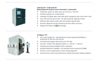
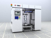
What is the advantage of the projection lithography instrument? It doesn't say what new features it has. The existing features of max wafer size, resolution, projection area, and overlay accuracy are not particularly impressive either, especially considering existing iline and KrF instruments.View attachment 105337
View attachment 105338
View attachment 105336View attachment 105339
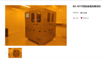
Early projection stepping lithography machine and nanoimprint lithography apparatus. created by CAS.
You are using an out of date browser. It may not display this or other websites correctly.
You should upgrade or use an alternative browser.
You should upgrade or use an alternative browser.
Chinese semiconductor industry
- Thread starter Hendrik_2000
- Start date
- Status
- Not open for further replies.
The resolution limit of the stepper is 1um, same capability as the most advanced SMEE SSB500 series.What is the advantage of the projection lithography instrument? It doesn't say what new features it has. The existing features of max wafer size, resolution, projection area, and overlay accuracy are not particularly impressive either, especially considering existing iline and KrF instruments.
the 50nm x 50nm field size is a bit less than 4 times the FE field size. The larger field size is for chiplet or interposer applications.
thus stepper is basically targeting for backend advanced packaging
The instrument is not particularly impressive even for packaging. Exposure size is slightly larger than SSB500 series in exchange for not being able to handle 300 mm wafers.The resolution limit of the stepper is 1um, same capability as the most advanced SMEE SSB500 series.
the 50nm x 50nm field size is a bit less than 4 times the FE field size. The larger field size is for chiplet or interposer applications.
thus stepper is basically targeting for backend advanced packaging
I also don't see any innovative features like UV LED source, maskless, dual stage, etc to reduce cost and increase efficiency for the end user. What is the significance of this instrument other than being a SMEE competitor for the 200 mm packaging market?
I think maybe was a precursors research machine for SMEE packaging machines.What is the advantage of the projection lithography instrument? It doesn't say what new features it has. The existing features of max wafer size, resolution, projection area, and overlay accuracy are not particularly impressive either, especially considering existing iline and KrF instruments.
SMEE had a prototype for this long ago though. If they have problems with ArF, OK, at least they should be improving their iline and KrF instruments.I think maybe was a precursors research machine for SMEE packaging machines.
I think UV-LED is maybe used more in automated mask aligners, due the low energy of the LEDs, like contact and proximity ones, because the light path is shorter. SMEE machines are projection stepping machines and the light path is longer and lot of energy is lost in the optics, they need a powerful UV-light source. I think is an area that they should explored thought. CETC/SEMICORE is trying to get into this type of litho machines, probably using UV-LED.UV LED source


Currently they are working with the ICRD and others in that.at least they should be improving their iline and KrF instruments.
From my understanding, the UV LED is indeed weaker and has a larger emission area but is much more energy efficient, longer lasting, and because you can tailor the emission area, you can optimize optics for lower loss.I think UV-LED is maybe used more in automated mask aligners, due the low energy of the LEDs, like contact and proximity ones, because the light path is shorter. SMEE machines are projection stepping machines and the light path is longer and lot of energy is lost in the optics, they need a powerful UV-light source. I think is an area that they should explored thought. CETC/SEMICORE is trying to get into this type of litho machines, probably using UV-LED.
View attachment 105340View attachment 105341View attachment 105342
This is a lab scale example of a maskless UV LED setup at 365 nm using just a small 4W array.
Interesting project, there is definitely good advantages of using LED instead of Hg Lamps. I have been thinking about building a dynamic mask static exposure apparatus using a UV LCD masking screen and LED looks like good option due costs.From my understanding, the UV LED is indeed weaker and has a larger emission area but is much more energy efficient, longer lasting, and because you can tailor the emission area, you can optimize optics for lower loss.
This is a lab scale example of a maskless UV LED setup at 365 nm using just a small 4W array.
But instead of developing 2 Arf dry machines, with the 2 different lens system for 90nm and 65nm resolution, SMEE is not developing a 65nm dry system (havoc confirmed it) and, maybe due to the very huge time pressure, decided to bite the bullet: the new 65nm setup goes directly to immersion!
So SMEE is developing an Arf dry machine at 90nm resolution and an Arf immersion machine at 38/45nm resolution, taking the 65nm optical setup and adding the immersion sub-system.
This is quite a brave step from SMEE. They are going with 2 untested new big innovations together in one go: the new 65nm resolution lens system immediately applied to the new immersion technology.
lol.. China. Pour more money into semiconductor tools, please.
其实就是没钱,所以没立项。把有限的钱用到最要紧的项目上
In fact, there was no money, so the project was not approved. Use limited money on the most important projects
- Status
- Not open for further replies.
