Chinese semiconductor industry

Status
Not open for further replies.

european_guy

Junior Member
Registered Member
If can guess what is happening is:
- The US want a ban in the entire ASML immersion line.

I also think so

-The US want ASML to stop servicing immersion machines in China.

IMHO this will not happen because is a savage move, hardly an European firm will act in such a barbarian way. If it happens it means US totally owns Europe.

-The US wants the Netherlands and Europe in general to adopt the same US person rule that they adopted.

This is illegal in Europe....probably is illegal also in US, but in Europe laws can not be bend to political will so easily. In Europe judges are not elected by politicians and of course cannot be removed/fired by politicians, so the Justice system is really an independent branch, not just on paper. This is not a small difference.
 
Last edited:

olalavn

Senior Member
Registered Member
Microgate Technology: The BAW filter has been packaged and can be replaced with domestic products. The company's BAW filter has completed the B41 FULL (main frequency range) product package and is performing performance tuning based on the test results. The agency predicts that the company will form a mass production scale of 10-20 million units per month by 2023
b0a79ab3gy1ha6kbppr7zj20wq0l1h54.jpg
 

european_guy

Junior Member
Registered Member
4. SSA800 dry Arf capable of 65nm resolution, for critical layers down to 55nm node. Not clear if this machine has been shipped already. Rumors say IRCD is testing a fully localized line for 55nm node. If rumor is confirmed, this probably is the machine used.

Havoc writes

上微没有65nm分辨率的光刻机,只有90nm分辨率的。90nm的有600和800两个型号

"Shangwei does not have a 65nm resolution lithography machine, only 90nm resolution. 90nm has two models of 600 and 800"

So it seems the dry Arf system has 90nm resolution, not 65nm as I wrote before in my summary, but it should be enough for a 55/65nm node.

Please be aware that machine resolution and corresponding chip node are different concepts.

I still wait if new info emerge, then I will update and repost my summary on SMEE 800 series.

U-precision dual-stage working station for dry-type machine

View attachment 105267

Havoc posted the above picture and at teh same time said:

能。下图是华卓招股书中提到的已量产并交付了10台的干式磁浮双工件台

That Google translate as "the dry-type dual-stage wafer table has been mass-produced and delivered 10 units"
 

hvpc

Junior Member
Registered Member
Havoc writes

上微没有65nm分辨率的光刻机,只有90nm分辨率的。90nm的有600和800两个型号

"Shangwei does not have a 65nm resolution lithography machine, only 90nm resolution. 90nm has two models of 600 and 800"

So it seems the dry Arf system has 90nm resolution, not 65nm as I wrote before in my summary, but it should be enough for a 55/65nm node.

Please be aware that machine resolution and corresponding chip node are different concepts.

I still wait if new info emerge, then I will update and repost my summary on SMEE 800 series.
90nm resolution is not enough to support the most critical layers in 65nm design node.

also, it’s not easy to operate at the extreme end of the capability spectrum.

SSA600 has attributes of first generation 193nm ArF scanners (0.75 NA). You’d need at least a second-gen (0.85 NA) or third-gen (0.93 NA) along with better k1 capabilities to support 65nm node and 55nm node.
 

european_guy

Junior Member
Registered Member
This is another very interesting piece of information, it is in the havoc thread, but not from havoc, so maybe it is to be confirmed

按分辨率区别,DUV光刻机有90干式,65干式,38~45浸没式。
90干式经济工艺节点130至65。
65干式经济工艺节点65至45。
38~45浸没式经济工艺节点45至22,多套刻几下也能达7,但无法商用,成本太高。
有了浸没式也意味着解决了65干式镜头组,65干式镜再加水浸没,由1.44折射率产生38~45nm分辨率,也就是浸没式。
如果楼主说的属实,则是65干式镜头组都用于浸没式了,没生产65光刻机。

"According to the difference of resolution, DUV lithography machine has 90 dry type, 65 dry type, and 38~45 immersion type.
90 dry economy process nodes 130 to 65.
65 dry economy process nodes 65 to 45.
38~45 submerged economical process nodes 45 to 22, can reach 7 with a few sets of engraving, but it cannot be commercialized, and the cost is too high.
The immersion type also means that the 65mm dry lens group is solved, and the 65mm dry lens is submerged in water, and the resolution of 38~45nm is produced by the 1.44 refractive index, that is, the immersion type.
If what the poster said is true, the 65 dry lens group is used for immersion, and no 65 lithography machine is produced."

I summarize according to what I have understood:

SMEE Arf 193nm has 2 setups / lens systems.

One setup has 90nm resolution 0.75NA, and the other has 65nm resolution (possibly because of a bigger second-gen 0.85 NA).

Relation between resolution and light source is given by
Please, Log in or Register to view URLs content!
: Resolution = k1 • λ / NA

But instead of developing 2 Arf dry machines, with the 2 different lens system for 90nm and 65nm resolution, SMEE is not developing a 65nm dry system (havoc confirmed it) and, maybe due to the very huge time pressure, decided to bite the bullet: the new 65nm setup goes directly to immersion!

So SMEE is developing an Arf dry machine at 90nm resolution and an Arf immersion machine at 38/45nm resolution, taking the 65nm optical setup and adding the immersion sub-system.

This is quite a brave step from SMEE. They are going with 2 untested new big innovations together in one go: the new 65nm resolution lens system immediately applied to the new immersion technology.
 
Last edited:

tokenanalyst

Brigadier
Registered Member

Weihua Technology and Southern Technology jointly build an advanced optical material testing laboratory to seize the third-generation semiconductor testing and analysis market​


Weihua Technology (TWSE: 3055), a professional brand of semiconductor testing solutions, and Southport Corporation, an emerging brand of digital optics, announced the expansion of cooperation, and a three-party alliance with Richang Optoelectronics to jointly create an "advanced optical material testing laboratory" to provide professional optical testing services . The laboratory will be officially opened in Linkou, Taiwan in February 2023. The first phase plans to provide non-destructive 3D material defect detection and 3D stress detection and analysis services for third-generation semiconductors. Perovskite, 2D materials, MicroLED, etc. will be gradually expanded in the future. Optical detection and analysis energy in the fields of materials and biomedicine.

With the rapid development of industrial technology, the challenges of semiconductor process and material technology development are increasing day by day. In particular, the research and development of new materials and new processes requires timely and corresponding new detection technologies to accelerate process development and verify the effectiveness of introduction. Promote the continuous growth of the industry. In addition, the current academic and research environment is also due to various factors such as the continuous increase in government subsidy thresholds and requirements, the decline in resource allocation and the quality of graduate students, and the many constraints on the equipment resources of Gongyi, making it difficult to improve the innovation, speed, and quality of research work.

727309079669.1204253249747725.65662.jpg


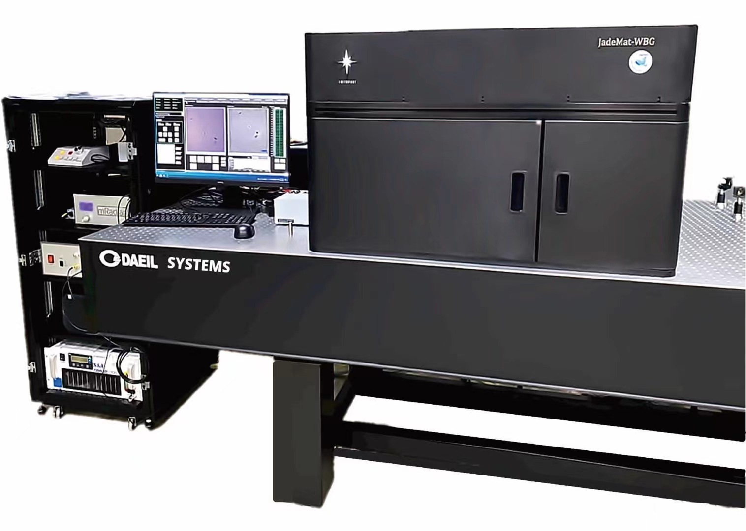
Weihua Technology and Southern Technology jointly build an advanced optical material testing laboratory, using JadeMat-WBG equipment to provide professional third-generation semiconductor optical testing services


Please, Log in or Register to view URLs content!
 
Status
Not open for further replies.
Top