Chinese semiconductor industry

Status
Not open for further replies.

tokenanalyst

Brigadier
Registered Member

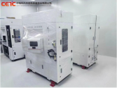
Semiconductor defect detection equipment Mars 4410 has been successfully shipped! China Electronics Technology Co., Ltd. escorts the development of my country's third-generation semiconductor industry​


Recently, CETC Fenghua Information Equipment Co., Ltd. launched the first third-generation semiconductor wafer defect detection equipment with completely independent intellectual property rights—Mars 4410. At present, the equipment has been sent to many domestic customers for use.
1673529528595.png
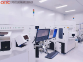
Mars 4410 is the key equipment in the silicon carbide device production line, used for defect detection of silicon carbide substrate wafers, epitaxial wafers, and corrosion wafers. After two years of unremitting efforts, the design team has overcome the core key technologies of optical detection such as laser scattering and microscopic imaging.

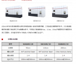
The equipment adopts various inspection methods such as differential interference phase contrast, photoluminescence, and dark field. Wafer inspection can be processed in parallel with data analysis. Wafer defects can be associated with device failure. It has low noise and high-resolution imaging, and high detection The advantages of throughput, high detection rate and accuracy can meet the needs of improving the yield of SiC devices.
1673529615627.png
Under the support and guidance of national, provincial and municipal industrial policies, CETC Fenghua has accelerated technological research, launched silicon carbide defect detection equipment, filled the domestic gap, broke international monopoly, realized import substitution, and actively responded to the urgent need for the development of my country's third-generation semiconductor industry. demand, and solved the "stuck neck" technical problem. China Electronics Technology Fenghua Company will continue to devote itself to the independent and localized construction of the industrial chain, and escort the independent controllable and high-quality development of my country's third-generation semiconductor industry!

Please, Log in or Register to view URLs content!
 

tphuang

Lieutenant General
Staff member
Super Moderator
VIP Professional
Registered Member
here are the updated TSMC utilization rate for Q1. Keep this in mind while we wait for SMIC earnings call and projections. Given its status as China's advanced node producer, it's utilization is likely to be a lot lower than what we are used to seeing. Demand from customers like Qualcomm, Unigroup are going to be low as long as global electronic industry is weak

Also from Tianjin's economic plans for 2023
做大做强制造业重点产业链。强化重大项目支撑,推动一汽丰田
Please, Log in or Register to view URLs content!
增产上量,中石化南港120万吨乙烯、华为天津区域总部等项目竣工,
Please, Log in or Register to view URLs content!
大二期、
Please, Log in or Register to view URLs content!
扩能、联想创新产业园、
Please, Log in or Register to view URLs content!
创新疫苗产业园等项目加快建设,渤化新材料产业园二期、卓朗工业软件产业园、海能发海洋装备制造等项目开工
SMIC 大二期 is listed there as a major project. Should see plenty of construction progress here.
 

tphuang

Lieutenant General
Staff member
Super Moderator
VIP Professional
Registered Member
News regarding Fujian Jinhua and Huawei

Please, Log in or Register to view URLs content!
From what I see. The key here are. This sounds like the Yandong micro production line.
目前中國尚無能力完全以中國半導體設備組成產線,「北京的唯一一條國產線,產量相當小。」
and here, the goal here is produce 20 to 28 nm chips at this PXW plant. People should relax about their dream of it producing CPUs for Huawei. If Huawei gets any domestic produced CPUs, it will be from SMIC
這家公司2021年6月才成立,由深圳市政府出資,要做20到28奈米晶圓代工業務,主要大客戶將是華為。
 

tokenanalyst

Brigadier
Registered Member
I re-checked ATP spec for SSB800 & XT400, they were both spec'ed at 280nm. The lower k1 for these scanners versus Canon's iLine stepper now makes more sense.
Make / ModelResolution (nm)k1wavelength (nm)NALitho Type
SMEE SSB8002800.503650.65Scanner
ASML XT4002800.503650.65Scanner
Canon FPA5550/iZ23500.553650.57Stepper
SMEE SSC8001100.362480.82Scanner
ASML XT8601100.352480.80Scanner
Canon FPA6300/ES6A900.312480.86Scanner
ASML XT1060800.302480.93Scanner
SMEE SSA600900.351930.75Scanner
ASML 5500/1150C900.351930.75Scanner
ASML XT1460650.311930.93Scanner
ASML NXT1470570.271930.93Scanner
1673534275427.png
The 800 series hadn't been officially announced yet.
 

european_guy

Junior Member
Registered Member
and here, the goal here is produce 20 to 28 nm chips at this PXW plant. People should relax about their dream of it producing CPUs for Huawei. If Huawei gets any domestic produced CPUs, it will be from SMIC

IMHO it makes sense for Huawei to keep buying US CPU and chips as long as is possible, this is also an indirect way to defend itself from further US attacks. If US companies do billions of $ out of Huawei, this has a value at lobbying level in Washington. Nobody knows if it will be enough, but has a value for sure.

It is telling that US has forbidden everybody from selling to Huawei...but their companies: Qualcomm, Intel, Micron, etc sell a lot of $ to Huawei, and are the only ones that got a license! No Koreans, no Taiwan. For instance IIRC only Micron sells DRAM and only Qualcomm (no Mediatek) sells smartphone chips for Huawei smartphones. It is real mafia!

OTH Huawei is pushing on localization of 5G gear, especially for base stations and telecom infrastructure, that is the most strategic and its traditional core business....and also easier to manufacture, it does not require super advanced nodes.
 
Last edited:

tokenanalyst

Brigadier
Registered Member
IMHO it makes sense for Huawei to keep buying US CPU and chips as long as is possible, this is also an indirect way to defend itself from further US attacks. If US companies do billions of $ out of Huawei, this has a value at lobbying level in Washington. Nobody knows if it will be enough, but has a value for sure.

It is telling that US has forbidden everybody from selling to Huawei...but their companies: Qualcomm, Intel, Micron, etc sell a lot of $ to Huawei, and are the only ones that got a license! No Koreans, no Taiwan. For instance IIRC only Micron sells DRAM and only Qualcomm (no Mediatek) sells smartphone chips for Huawei smartphones. It is real mafia!

OTH Huawei is pushing on localization of 5G gear, especially for base stations and telecom infrastructure, that is the most strategic and its traditional core business....and also easier to manufacture, it does not require super advanced nodes.
Same thing ASML complained about, while they were banned from selling EUV Low NA tools to China, US semiconductor tool makers were getting licenses to sell their best gear.
 

tphuang

Lieutenant General
Staff member
Super Moderator
VIP Professional
Registered Member
View attachment 104931
The 800 series hadn't been officially announced yet.
Right, I was going to say that. 800B/C according to Havok has not been validated anywhere (not sure if it has started testing), so we don't know how adequate it might be. SS_600 series is clearly not commercially competitive. One should not use that series of lithography machines to judge the commercial competitiveness of 800 series.

From what we are hearing, sounds like SSA800 dry will be able to do 65nm on single exposure (according to Havok), so it will be quite an improvement over SSA600 which can only do 90nm. This would indicate 55nm line for ICRD is likely doing multiple exposures with SSA800 and also able to do this will SMEE iLine/krf scanners (maybe SSB/C600). When this does get validated, I think it indicates that SMEE scanners are commercially competitive for at least 55 to 90nm production.
 
Last edited:

european_guy

Junior Member
Registered Member
SMEE does share more info with their customers ranging from product introduction to ATP Specifications. Just because you dont have access to info on SSx800 series scanners doesn’t mean I don’t.

Havoc is not the only one that has access to info on SMEE beyond what’s on their website.

by the way, I shared that table/info to answer @FairAndUnbiased’s question on the delta resolution capability between SMEE and ASML. He mentioned the 90nm resolution for ArF, so I specifically relayed info pertaining to why SSA600 resolution limit was set at 90nm. I wasn’t trying to judge SSA800’s commercial viability via comparison to SSA600. But, I think it is reasonable to extrapolate SSA800 readiness based on progress or lack thereof of SSB800 and SSC800.

So according to your info and getting also info from havoc, I try here to tentatively put together the pieces of this puzzle.

Here are the new SMEE litho machines.

1. SMEE new platform is a double wafer stage type and is named 800 series. This series totally replaces the obsolete 600 series.

2. Of this new 800 series, according to havoc and to your table, 2 machines are already in volume production (although no info on customers, delivered numbers, etc): the SSB800 i-line (365nm) capable of 280nm resolution, and the SSC800 KrF (248nm) capable of 110nm resolution

3. There is also at some customer's site, like IRCD, for testing and validation purposes, but still not in volume production, the SSA800 Arf (193nm) capable of 55/65nm resolution (it seems IRCD is testing a 55nm line).

4. There is also a prototype version at SMEE's site of the still unnamed Arfi (193nm immersion) capable of 28nm resolution. This latest machine is expected to be delivered to selected customers for validation within this year.


Can someone confirm/correct the above summary?
 

hvpc

Junior Member
Registered Member
So according to your info and getting also info from havoc, I try here to tentatively put together the pieces of this puzzle.

Here are the new SMEE litho machines.

1. SMEE new platform is a double wafer stage type and is named 800 series. This series totally replaces the obsolete 600 series.
Yes
2. Of this new 800 series, according to havoc and to your table, 2 machines are already in volume production (although no info on customers, delivered numbers, etc): the SSB800 i-line (365nm) capable of 280nm resolution, and the SSC800 KrF (248nm) capable of 110nm resolution
Only 1 SSB800 iLine scanner has been shipped to SMEE “customer” last September. It’s still not in production as of today. Like I said, many critical features are missing so the fab’s target application will be for the least critical layers with very loose specification/tolerance. Initial target applications would be for the polyamide or for the implant layers for memory fabs to test out SMEE SSB800 machines. SMEE is having trouble shipping the 2nd SSB800 iLine scanner

SMEE is also having trouble with shipping the first SSC800 KrF scanner.
3. There is also at some customer's site, like IRCD, for testing and validation purposes, but still not in volume production, the SSA800 Arf (193nm) capable of 55/65nm resolution (it seems IRCD is testing a 55nm line).
First, resolution capability or half-pitch capability, does not have one-to-one correlation with the design/process node.

Assuming SMEE is really working on a 193nm dry SSA800, it’s more likely it will target 65nm resolution capability. Application for such tool would be for critical layers down to 55nm node.
4. There is also a prototype version at SMEE's site of the still unnamed Arfi (193nm immersion) capable of 28nm resolution. This latest machine is expected to be delivered to selected customers for validation within this year.
The 193nm immersion resolution capability would be 38nm. with everyone indicating this scanner is to be equivalent to ArFi used for 28nm, the target specifications would mimic ASML’s NXT1950.
 
Last edited:
Status
Not open for further replies.
Top