Chinese semiconductor industry

Status
Not open for further replies.

tinrobert

Junior Member
Registered Member
Thanks. @tinrobert is a great source. Although, I'd point out that Information Network probably didn't get all the new fabs that are coming online. Still, his over point is probably accurate enough. We will just have to wait and see how much they really increase.


yep, like I posted here
KLA/AMAT/LAM 2023 projections are way too optimistic about revenue in China is way too optimistic. Considering that Koreans and Taiwanese are not allowed to expand production in China after taking money from CHIPS act,, I'm not sure how they don't lose like 80 to 90% of their revenue from the China market.


meh, I think we discussed this extensively. The original article about $143 billion didn't make a lot of sense. They will have a very thorough and holistic approach to this. Just putting a dollar sign on it doesn't make sense. The Chinese IC sector already gets so much benefit from the local gov't.
"Thanks. @tinrobert is a great source. Although, I'd point out that Information Network probably didn't get all the new fabs that are coming online. Still, his over point is probably accurate enough. We will just have to wait and see how much they really increase."
Yes you are correct. In my newsletter to subscribers (this article published is an abridged "free" version, I have more details of each of these fabs. In addition, I have more data on more fabs, but I don't want to give away too much free stuff, as I sell my reports, which can be seen on my website at
Please, Log in or Register to view URLs content!
 

tokenanalyst

Brigadier
Registered Member
People here have a lot confidence in this havok guy, but something tells me that Havok is just reciting the U-Precision IPO documents from June 2021, when U-Precision was in the R&D phase the firsts prototypes of the maglev wafer stage, public information that we posted here and nothing in his posts looks different of the things we having posting here, since 2021 or things you can find on your own in the Chinese internet.
I usually avoid posting from social media including Chinese social media, preferring to go official or semiofficial sources like semiconductor related new sources, patents, research papers, research institutions postings, companies postings and so on. But with the confident that people have here maybe is someone related to the project who knows, but for some reason I personally find that his post are not different of the ones we have been posting here. IDK my personal opinion.
1672888631755.png
He posted that in December 24.

While here is the same post is from June 2022
development ultra high precision heterodyne interferometry and its use in precision measurement instruments like lithography machines and LIGO type instruments (to measure hecking black holes collision).

Of ultra-precision high-speed laser interferometric displacement measurement technology and instruments.​


In response to the ultra-precision and high-speed displacement measurement requirements put forward in high-end equipment such as microelectronic lithography machines, Harbin Institute of Technology has deeply explored the traditional common optical path heterodyne laser interferometry method and a new generation of non-common optical path heterodyne laser interferometry methods. It has made continuous breakthroughs in many key technologies such as high-precision laser frequency stabilization, precise suppression of optical nonlinear errors, high-speed and high-resolution interference signal processing, and has developed a series of ultra-precision high-speed laser interferometers with the highest relative accuracy of laser vacuum wavelength. 9.6×10 -10 , the displacement resolution is 0.077 nm, the minimum optical nonlinearity error is 13 pm, and the maximum measurement speed is 5.37 m/s. At present, this series of instruments has been successfully used in the field of integrated development and performance testing of lithography machine prototypes with multiple process nodes from 350 nm to 28 nm in my country, providing key technical support and important measurement methods for the development of high-end equipment such as lithography machines in my country.

View attachment 90032

-Testing in litho machines

4.1 Development of domestic lithography machine: multi-axis high-speed ultra-precision laser interferometer​


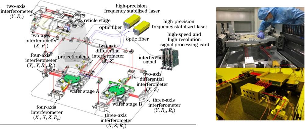
In the development of domestic lithography machines, the multi-axis high-speed ultra-precision laser interferometer is one of the core units embedded in the lithography machine and determines its lithography accuracy. However, on the one hand, European and American countries clearly stipulated that this type of interferometer products are strictly embargoed to my country in the Wassenaar Agreement; Development and production of domestic lithography machines. To this end, our research group has developed a series of ultra-precision high-speed laser interferometry systems, which have been successfully applied in the field of integrated development and performance testing of lithography machine prototypes with multiple process nodes from 350 nm to 28 nm in my country. Typical applications such asFigure 18As shown in the figure, all its key indicators meet the research and development needs of domestic advanced lithography machines, break the embargo blockade imposed by foreign related products on my country, and play an important role in the development of domestic lithography machines. In the applied lithography machine, the number of measurement axes of the interferometer can reach more than 22 axes, the maximum measurement speed can reach 5.37 m/s, and the laser vacuum wavelength/frequency accuracy can reach up to 9.6 × 10 -10 ( k = 3 ), the displacement resolution can reach 0.077 nm, and the minimum optical nonlinearity error is 13 pm. With the ultra-stable constant temperature air bath (3~5 mK@10 min) and vibration isolation environment, the linear displacement and angular displacement can be measured and decoupled synchronously for the multi-dimensional motion of the double workpiece stage in the lithography machine to meet the requirements of the mask. The increasingly complex relative position/attitude measurement requirements between the workpiece table, the silicon wafer workpiece table and the projection objective lens, thereby ensuring the overall overlay accuracy of the lithography machine.​

Schematic diagram of application of ultra-precision high-speed laser interferometry system in lithography machine and field photo

Figure 18. Application principle and on-site photo of ultra-precision high-speed laser interferometry system in lithography machine​

Fig. 18. Schematic diagram of application of ultra-precision high-speed laser interferometry system in lithography machine and field photo​


-Testing in some precision measuring instrument

4.2 Development of National Metrology Benchmark Device: Sub-nanometer Precision Laser Interferometer​


In the development of national-level measurement reference devices, how to use basic physical constants to redefine the mass unit kilogram has been rated as one of the six major scientific problems in the world in recent years by the internationally renowned academic journal "Nature". In the "energy balance" scheme proposed by Academician Zhang Zhonghua of the Chinese Academy of Metrology, one of the key points is to use an ultra-precision laser interferometer to achieve high-accuracy length measurement, which requires an absolute measurement accuracy of less than 1 nm. To this end, our research group developed the first set of sub-nanometer laser interferometers in my country and successfully applied them to the first set of quantized quality benchmark devices in China (Figure 19), played a key role in the implementation of the Chinese scheme of quantized mass benchmarks, and promoted China to become one of the first six countries to successfully participate in the international comparison of kilogram
Please, Log in or Register to view URLs content!
[
Please, Log in or Register to view URLs content!
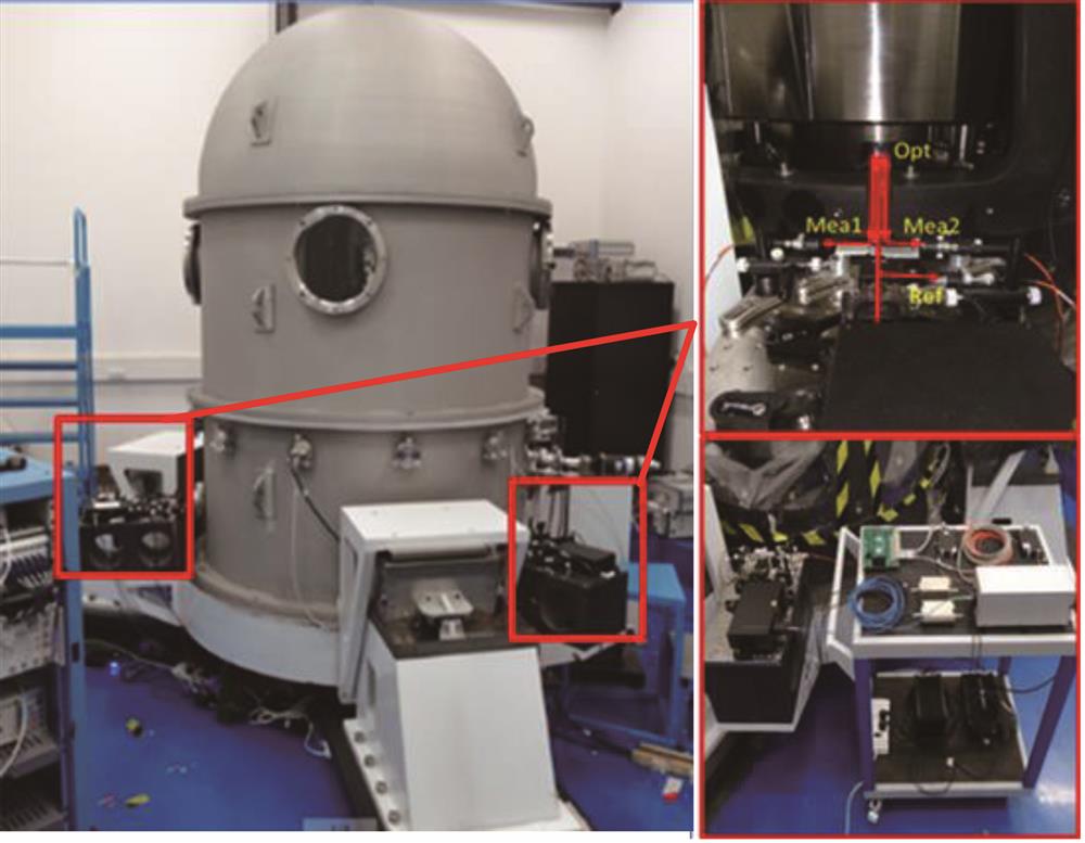
] . In order to achieve sub-nanometer measurement accuracy, in addition to the precise vibration isolation and temperature control environment, the laser interferometer must be measured in a vacuum environment to exclude the influence of air refractive index on the laser wavelength, and its measurement uncertainty can reach 0.54 nm. @100mm. In addition, in order to realize the attitude monitoring of the measured object, the number of measurement axes of the interferometer reaches 9 axes.

National quantized mass standard and integrated sub-nanometer interferometer

Figure 19. National Quantization Quality Benchmark and its integrated sub-nanometer laser interferometer​

Fig. 19. National quantized mass standard and integrated sub-nanometer interferometer​


Please, Log in or Register to view URLs content!
 

ZeEa5KPul

Colonel
Registered Member
People here have a lot confidence in this havok guy, but something tells me that Havok is just reciting the U-Precision IPO documents from June 2021
He supposedly works at SMEE, so he's the closest we have to a first hand source in this matter. It's even more opaque than the PLA, and that's really saying something - at least with them we get the occasional picture and interview. I don't think we should expect him to have any deep insight into what's going on at U-Precision, so it's reasonable to assume he's just reciting public knowledge.
 

tokenanalyst

Brigadier
Registered Member
He supposedly works at SMEE, so he's the closest we have to a first hand source in this matter. It's even more opaque than the PLA, and that's really saying something - at least with them we get the occasional picture and interview. I don't think we should expect him to have any deep insight into what's going on at U-Precision, so it's reasonable to assume he's just reciting public knowledge.
If that is correct then is someone important.
 

broadsword

Brigadier
Yeah, reading this article has calmed me down some, deliberately provocative headline aside
Please, Log in or Register to view URLs content!
Good to know that these pieces of trash (especially the Tsinghua Unigroup president and likely source of U-Precision's problems) are going to be thrown in prison. It really is a shame China got rid of its re-education through labour system; these people need to break rocks with pickaxes on a chain gang for the rest of their lives.

It's very reassuring to know that the government understands the scale of the problem and will tackle it. It reminds me of the PLA reforms circa 2015 when the PLA was shot through with corruption and Xi cleaned it up ruthlessly (a couple of PLA generals even offed themselves to avoid punishment, smartest thing they ever did). Look at it today, not even 10 years later - a night and day difference.

Unfortunately, a lot of time - the most valuable commodity - was lost. Still, better late than never and there have been some very recent encouraging developments. It seems SMEE intends to mass produce 28/22nm DUVi tools fairly soon and are already delivering (or will soon deliver) some beta versions to customers, so they have to be getting immersion workpieces from somewhere. They're already sanctioned so they're not getting them from the US. @tokenanalyst posted some patents relating to DUVi some time back, so I'd like to get his (and other knowledgeable members') sense on where U-Precision is at present.

To think some people here were arguing with me that corruption benefited the country. Or were they meant to say it benefited others but not China? LMAO.
 

tokenanalyst

Brigadier
Registered Member

Jiangfeng Electronics: The company's CMP product sales are in a continuous growth trend​

Jiangfeng Electronics stated on the investor interaction platform that the company has carried out a strategic layout in CMP (Chemical Mechanical Planarization), and the sales of CMP products are in a continuous growth trend.

Previously, Jiangfeng Electronics stated in an agency survey that the company's CMP products mainly include CMP retainer rings (Retainer Ring), polishing pads (Pad), activation disks (Disk) and CMP group head services, and its customers and integrated circuit targets The customers are basically the same. The company has introduced core talents who master the above technologies and markets to develop such products in an all-round way, and will provide customers with integrated services and solutions by virtue of its advantages in technology, service, and quality. At present, the company's CMP products have achieved mass production and delivery in many chip manufacturers and semiconductor equipment manufacturers.

Regarding the company's growth space, Jiangfeng Electronics said that with the surge in 5G connections, artificial intelligence, deep learning, virtual reality and other emerging applications in the mobile, data center and cloud computer servers, automotive and industrial markets, the upstream raw materials for chips have exceeded The demand for high-purity sputtering targets continues to grow. At the same time, in the face of the fast-growing domestic market, the company's precision parts and CMP business is facing a relatively favorable market environment and has a large room for growth.

Please, Log in or Register to view URLs content!
 

tonyget

Senior Member
Registered Member
The deeper I look into U-precision,the more dodgy this company appears. There is a reason why they got rejected listing by Shanghai stock exchange

Problems with U-precision

Please, Log in or Register to view URLs content!

First the Shanghai stock exchange questions U-precision,regarding their operation,especially dual-stage working station for lithography machine related info.

They didn't reply directly,instead they have filed a new listing request. This time they have deleted lithography machine related stuff in the listing file

Please, Log in or Register to view URLs content!
华卓精科再上会“挤水分”:招股书删除“光刻机”概念
U-precision "squeeze water" again: the prospectus deletes the concept of "lithography machine"

So what U-precision saying is that:regarding the infor for dual-stage working station for lithography machine,there is no confidentiality requirement by law nor by gov,but because of the "sensitive nature" of the project,they don't want to reveal the relevant progress to IPO office. I'm not sure the IPO office buy this excuse

发行人参与上述 02 专项研发任务未被纳入国家秘密保护范围,不属于保密项目,发行人对其名称、投入金额、研发进度等信息披露不违反《中华人民共和国保密法》、《国家科技重大专项(民口)资金管理办法》等法律法规的规定。

考虑到与纳米精度运动及测控系统相关的 02 专项,涉及国家相关领域信息敏感性。为保护国家相关领域敏感信息,在符合科创板发行上市信息披露要求的前提下,发行人对其内容进行豁免披露。

综上所述,发行人以满足科创板发行上市信息披露要求为原则,在保护国家相关领域敏感信息的情况下,对与纳米精度运动及测控系统相关的02专项名称信息、技术内容、研发进展、协议内容等信息进行豁免披露;发行人申请豁免披露后,发行人信息披露符合国家法律法规规定和科创板发行上市信息披露要求。

The issuer's participation in the above-mentioned 02 special research and development tasks is not included in the scope of state secret protection and is not classified as a confidential project. The issuer's disclosure of information such as its name, investment amount, and research and development progress does not violate the "Confidentiality Law of the People's Republic of China" and "National Major Science and Technology Projects". (Civil Population) Fund Management Measures” and other laws and regulations.

Considering the 02 special project related to nano-precision motion and measurement and control systems, it involves information sensitivity in related fields of the country. In order to protect sensitive information in relevant fields of the country, issuers are exempted from disclosing their contents, provided that they meet the information disclosure requirements for issuance and listing on the Science and Technology Innovation Board.

To sum up, the issuer shall comply with the information disclosure requirements for issuance and listing on the Science and Technology Innovation Board, and under the condition of protecting sensitive information in related fields of the country, the 02 special name information, technical content, research and development related to nano-precision motion and measurement and control systems progress, agreement content and other information are exempted from disclosure; after the issuer applies for exemption from disclosure, the issuer's information disclosure complies with the provisions of national laws and regulations and the information disclosure requirements for issuance and listing on the Science and Technology Innovation Board.

Please, Log in or Register to view URLs content!
关于北京华卓精科科技股份有限公司首次公开发行股票并在科创板上市的科创板上市委会议意见回复
Reply to the opinions of the Science and Technology Innovation Board Listing Committee meeting of Beijing U-precision Technology Co., Ltd. for its initial public offering and listing on the Science and Technology Innovation Board

Please, Log in or Register to view URLs content!
关于北京华卓精科科技股份有限公司首次公开发行股票并在科创板上市申请文件第二轮审核问询函的回复
Reply to the Inquiry Letter on the Second Round of Review of Beijing U-precision Technology Co., Ltd.’s IPO and Listing Application Documents on the Science and Technology Innovation Board
 

tacoburger

Junior Member
Registered Member
The way I see it, China's semiconductor industry is surviving. But it's not enough. SMIC is meant to be China's answer to TSMC, are they really gonna to be happy with mass production of 28nm/14nm chips and extremely limited production of 7nm, even if it's all done with entirely domestic equipment.? And it seems that America purposely doesn't target the low end chips for this reason, they said it themselves, "I don't care about the chips that they use in the airbags of cars". The sanctions are meant to slow down the high end chip development and it has succeeded.

By the time SMIC can get access to EUV in 2025-2030, who knows what node size TSMC and Intel are up to, or if they're even planning to shift to an entirely new architecture and/or material other than silicon to get them below or faster than 1nm. And keep in mind that even by some miracle that the EUV is in mass production by 2025 and SMIC gets like a dozen of them, it could take 1-2 years for them to figure out how to get mass production of sub 5nm chips, Intel has EUV for years and hasn't figured it out 5nm. And this is important years, A.I is developing so fast, a reduction in computing power now could meant a massive lack of progress in A.I development compared to America.

I hope that China's semiconductor industry isn't so focused on surviving and producing "low end chips" that they miss whatever new revolution that will bring us faster computing on a sub 1nm node and have to catch up all over again.

Hell it seems like foresight is a major issue with the semiconductor industry. Huawei 2018 and the EUV ban should have been a wake up call for the entire industry but most firms still went ahead with American chips and equipment. Even the massive subsidies and loans that the government gave the industry went into Fabs and design firms instead of the glaring weakness of semiconductor equipment sector. The EDA and most recent equipment ban seemed like a massive shock to the industry but really shouldn't have been, seeing how bad the relationship between Washington and Beijing is.

SMEE and other semiconductor equipment should have been treated like a wartime scenario of total national importance since the 2018 bans, but instead it's seems like it's only happening now, after the latest rounds of sanctions. I really have no idea what's going on in the heads of top level industry leaders to not expect this level of attack, the sanctions of Russia in early 2022 were an early warning of how much pressure America and her allies can apply if need be, even if it hurts them badly.

And America could do a lot more if they wanted to, even if it means hurting themselves. I hope that they have a plan if America goes for another round of sanctions or goes full scorched earth and puts the entire semiconductor industry on the same level of sanctions as Russia faces, aka, total cessation of all sales of material and equipment to China and a total ban on semiconductors from China.
 

mmbro

New Member
Registered Member
Maybe?

"Lee calls this dynamic one of the more interesting trends that may come out of the current fight over chip controls. “A lot of this capacity is already in China. Most of the new capacity at these [mature] nodes is being built in China, and there’s a limited capacity [of chipmaking equipment supply], even if the money and the political will is there to develop this in the US and EU,” Lee says. The footprint of China in “supplying the more mundane, high-volume, lower-margin, lower-sophistication, but still indispensable chips,” he adds, “is becoming bigger rather than smaller.”


Please, Log in or Register to view URLs content!
 

ansy1968

Brigadier
Registered Member
The way I see it, China's semiconductor industry is surviving. But it's not enough. SMIC is meant to be China's answer to TSMC, are they really gonna to be happy with mass production of 28nm/14nm chips and extremely limited production of 7nm, even if it's all done with entirely domestic equipment.? And it seems that America purposely doesn't target the low end chips for this reason, they said it themselves, "I don't care about the chips that they use in the airbags of cars". The sanctions are meant to slow down the high end chip development and it has succeeded.

By the time SMIC can get access to EUV in 2025-2030, who knows what node size TSMC and Intel are up to, or if they're even planning to shift to an entirely new architecture and/or material other than silicon to get them below or faster than 1nm. And keep in mind that even by some miracle that the EUV is in mass production by 2025 and SMIC gets like a dozen of them, it could take 1-2 years for them to figure out how to get mass production of sub 5nm chips, Intel has EUV for years and hasn't figured it out 5nm. And this is important years, A.I is developing so fast, a reduction in computing power now could meant a massive lack of progress in A.I development compared to America.

I hope that China's semiconductor industry isn't so focused on surviving and producing "low end chips" that they miss whatever new revolution that will bring us faster computing on a sub 1nm node and have to catch up all over again.

Hell it seems like foresight is a major issue with the semiconductor industry. Huawei 2018 and the EUV ban should have been a wake up call for the entire industry but most firms still went ahead with American chips and equipment. Even the massive subsidies and loans that the government gave the industry went into Fabs and design firms instead of the glaring weakness of semiconductor equipment sector. The EDA and most recent equipment ban seemed like a massive shock to the industry but really shouldn't have been, seeing how bad the relationship between Washington and Beijing is.

SMEE and other semiconductor equipment should have been treated like a wartime scenario of total national importance since the 2018 bans, but instead it's seems like it's only happening now, after the latest rounds of sanctions. I really have no idea what's going on in the heads of top level industry leaders to not expect this level of attack, the sanctions of Russia in early 2022 were an early warning of how much pressure America and her allies can apply if need be, even if it hurts them badly.

And America could do a lot more if they wanted to, even if it means hurting themselves. I hope that they have a plan if America goes for another round of sanctions or goes full scorched earth and puts the entire semiconductor industry on the same level of sanctions as Russia faces, aka, total cessation of all sales of material and equipment to China and a total ban on semiconductors from China.
Hi and welcome to the forum, while you opinion are commendable, I advise you to look at what Liang Mong Song had stated on his resignation letter to the SMIC board. He said that SMIC's 7nm node has already completed full development, and is preparing mass production April 2021. More surprisingly, the designs and most of the development for 5nm and 3nm nodes have already been mostly completed.

The following is the full text of Liang Mengsong's resignation:

Letter to the Board of Directors

Hello, chairman and directors!

I know that we will make a very important personnel appointment decision at this meeting today.

Currently,
Please, Log in or Register to view URLs content!
is facing various pressures from the United States, leading to serious threats to the development of advanced technology. I believe that today's personnel proposal will inevitably affect the company's prospects.

It has been more than three years since I was appointed as the co-CEO by the board of directors in November 2017. In these more than 1,000 days, I almost never took a vacation. Even in June 2019, when I was experiencing life At the most dangerous moment, I never gave up, and I never let you down.

During this period, I tried my best to complete five generations of technology development from 28nm to 7nm. This is a task that an average company takes more than ten years to accomplish. And these results are obtained by more than 2,000 engineers led by me, working hard day and night. Of course, the trust and support of the chairman and the directors in the past is also a key element of success.

I originally came to mainland China not to seek high-ranking officials, but simply to contribute to the mainland's high-end integrated circuits. At present, 28nm, 14nm, 12nm, and n+1 technologies have all entered mass production, and the development of 7nm technology has also been completed. Risk mass production will be available in April next year. The 8 most critical and most difficult technologies of 5nm and 3nm have also been carried out in an orderly manner. Only when the EUV lithography machine arrives, we can enter the full development stage.

It seems that my short-term goal seems to have exceeded expectations and was successfully achieved.

I received a call from the chairman of the board on December 9th, last Wednesday morning: Mr. Jiang is about to become the vice chairman of the company. I was very surprised and puzzled about this, because I didn't know anything about it beforehand. I deeply feel that I am no longer respected and distrusted. I think you should no longer need me here to continue to work hard for the company's prospects. I can rest for a while.

After the company’s board of directors and shareholders’ meeting have approved Mr. Jiang’s nomination, I will formally submit my resignation. But the company should give a comprehensive and fair evaluation of my contribution over the past three years, and I should have the right to accept and appeal.

I solemnly tell you that I do not have the slightest intention to influence your next vote on this personnel appointment, but I think I should let everyone know my true feelings.

My statement hopes that Ms. Guo Guangli, secretary of the board of directors, can be included in the official meeting minutes of this interim board of directors.

Thank you all.


As the letter stated SMIC had mapped out the development of 5nm and 3nm Chips, so they needed an EUVL to verify their progress, BUT there are other tools available like the SSRF in Shanghai and I'm certain that they are testing the mask and photoresist so when a viable Chinese EUVL come on line in late 2024 and early 2025 both chips are production ready. I also speculate by 2025 both China and the US are in a same boat regarding 5nm chips (SMIC 5NM N+3 DUVL) unless TSMC relent and produce their 3nm chips in Arizona.
 
Status
Not open for further replies.
Top