his entire post had 0 question marks in it. I only saw declarative statements.you both just tell the importance of old end/mid end chips. but still didn't reply to his actual question. XD
@ansy1968 posted with details.
SMIC already begun 5nm and 3nm R&D back in 2020. just awaiting EUV machines.
Liang's letter indicated that SMIC has completed R&D for 7-nm technologies and is expected to enter risky mass production in April 2021, while the R&D for eight key technologies for 5-nm and 3-nm chip products has started, but it is awaiting EUV lithography machines to conduct comprehensive development.
You are using an out of date browser. It may not display this or other websites correctly.
You should upgrade or use an alternative browser.
You should upgrade or use an alternative browser.
Chinese semiconductor industry
- Thread starter Hendrik_2000
- Start date
- Status
- Not open for further replies.
lmao... everyone knows China has started from zero since the epidemic came.. give them time from here to 2027... U.S is not confident enough to face "chip war" after 2024...you both just tell the importance of old end/mid end chips. but still didn't reply to his actual question. XD
@ansy1968 posted with details.
SMIC already begun 5nm and 3nm R&D back in 2020. just awaiting EUV machines.
Liang's letter indicated that SMIC has completed R&D for 7-nm technologies and is expected to enter risky mass production in April 2021, while the R&D for eight key technologies for 5-nm and 3-nm chip products has started, but it is awaiting EUV lithography machines to conduct comprehensive development.
now they aren't confident enough, let alone 2024.
Yes sir By that time the Chinese had transform itself from a rag tag guerilla outfit to a modern army ready to take the fight to the Americans and 2025 will be the date of reckoning, I imagine it will be like the Huaihai campaign overwhelming the American from the matured node and outpricing them in leading edge.lmao... everyone knows China has started from zero since the epidemic came.. give them time from here to 2027... U.S is not confident enough to face "chip war" after 2024
@olalavn Sir you will like this from SMIC Ningbo with love. 
6 minutes agoNew

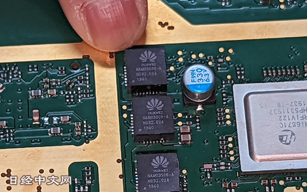
First time I have seen a Huawei logo chip. Its a power management chip.
My guess is by the newly acquired SMIC ningbo which specialized in analog, power management.
First step to become IDM.
Oldschool
Junior Member
Registered Member6 minutes agoNew

First time I have seen a Huawei logo chip. Its a power management chip.
My guess is by the newly acquired SMIC ningbo which specialized in analog, power management.
First step to become IDM.
Dell is going full throttle on complete supply-chain decoupling from China
US computer giant Dell to replace all China-made chips in its products by 2024 amid tensions between Beijing and Washington
- Dell wants all of the chips used in its products, including those made by foreign suppliers in China, to be sourced from outside the country
- Dell reportedly also plans to move about 50 per cent of its production out of China by 2025
Personal computer (PC) giant Dell Technologies plans to stop using China-made semiconductors by 2024 and urged its suppliers to cut down on components sourced from that country amid concerns over escalating tensions between Beijing and Washington.
Dell’s goal is to have all of the chips used in its products, including those produced by foreign suppliers in China, to be sourced from outside the country by 2024, the report said.
Equation
Lieutenant General
But Dell can't replace China's processed rare Earth elements that makes those chips and ALL of the electronic parts.Dell is going full throttle on complete supply-chain decoupling from China
True. I guess they are going for complete high-tech supply chain decoupling thenBut Dell can't replace China's processed rare Earth elements that makes those chips and ALL of the electronic parts.
Somewhat advanced MCUs for cars. Like in car entertainment systems. SoCs for TVs and lower end set top boxes. But I think a lot of these applications will move to 28nm in due time. TVs are moving towards higher resolutions and the H.265 and AV1 codecs are becoming more prevalent.Wonder what the applications of the mid tier wafers (32-90 nm) will be. MCUs, power, analog, etc. can be done with super cheap KrF tools at 130+ nm. Once you get to <90 nm you have to use dry ArF, a step up in cost. From that list I see lots of automotive chip companies like CanSEMI and CR Micro.
No. But it is a matter of what you can do right now. Also, outside of mobile the current advantage of 5nm and better is kind of limited. With good chip design you can do well enough with 7nm. For example Intel has been able to remain competitive despite a two node disadvantage by having asymmetrical cores on their CPUs similar to ARM big.LITTLE.The way I see it, China's semiconductor industry is surviving. But it's not enough. SMIC is meant to be China's answer to TSMC, are they really gonna to be happy with mass production of 28nm/14nm chips and extremely limited production of 7nm, even if it's all done with entirely domestic equipment?
The low end chips often have much lower margins. But there are exceptions. For example Texas Instruments has consistently high margins despite making chips with comparatively obsolete technology. It depends on the market segment you are in.And it seems that America purposely doesn't target the low end chips for this reason, they said it themselves, "I don't care about the chips that they use in the airbags of cars". The sanctions are meant to slow down the high end chip development and it has succeeded.
No one knows what will happen after 1nm. This is the first time the sector has not had a clear roadmap that far ahead. So who knows.By the time SMIC can get access to EUV in 2025-2030, who knows what node size TSMC and Intel are up to, or if they're even planning to shift to an entirely new architecture and/or material other than silicon to get them below or faster than 1nm.
Intel dabbled in EUV initially but then they gave up on it. They focused on highly complex multiple-patterning schemes with DUV that no one else uses. And they failed hard at getting this to work. They wanted to skimp out on tool expenses and it bit them. Globalfoundries is stuck at 14nm for much of the same reasons. The extremely high cost of EUV tools means they are out of reach for a lot of businesses.And keep in mind that even by some miracle that the EUV is in mass production by 2025 and SMIC gets like a dozen of them, it could take 1-2 years for them to figure out how to get mass production of sub 5nm chips, Intel has EUV for years and hasn't figured it out 5nm.
I think AI is overrated. I am much more concerned with the introduction of GAA transistors which are claimed to have 50% less power consumption and be radiation resistant. Learning applications can be done in the back end in large facilities. And any AI applications in the field will use static databases and algorithms with much simpler to implement hardware.And this is important years, A.I is developing so fast, a reduction in computing power now could meant a massive lack of progress in A.I development compared to America.
They have no viable alternative so what do they want them to do. I do think the industry should have made a fund to work on Chinese tools but they have limited capital so the government has to do this.Hell it seems like foresight is a major issue with the semiconductor industry. Huawei 2018 and the EUV ban should have been a wake up call for the entire industry but most firms still went ahead with American chips and equipment.
The government invested quite a lot on the tools sector so this is not true. You could argue they should have invested even more but that is besides the point.Even the massive subsidies and loans that the government gave the industry went into Fabs and design firms instead of the glaring weakness of semiconductor equipment sector.
You are taking this Western news release way too seriously. China has been heavily investing in EDA for a couple of years already.The EDA and most recent equipment ban seemed like a massive shock to the industry but really shouldn't have been, seeing how bad the relationship between Washington and Beijing is.
POWER8 uses 22nm SOI process. It is not quite the same as bulk silicon.14-28 nm is already extremely capable for even logic at 20+ nm as shown by IBM Power8
Between the desktop apocalypse now that the lockdowns are over, and the server apocalypse now that large consumers of servers like Amazon are moving towards designing their own chips and systems, plus the move towards cloud services, either Dell focuses on laptops or they are dead meat.
- Is probably is going to be expensive to Dell. But they could pass the cost to their consumers.
-That "diversification" thing is not news, in 2014 every single news pundit was talking to move the supply chains to outside China and that when nowhere because as manufacturing started to move out the Chinese dropped their prices to be even more attractive.
-Dell is the second PC seller in China, wouldn't be funny that Chinese pass a law demanding that all PCs, laptops, smartphones, etc sold in China use a least 50% Chinese made chips or more. "be careful what your wish for", they either drop out of the Chinese market or divide their supply chain in two and absorb the cost.
They don't really buy a lot of Mainland Chinese chips, disarm any Dell product and most of their Chips are from Taiwan probably more than 80% made in Taiwan. Most of the chips made in Mainland China are for internal consumption, including the ones made by foreign companies. Probably one or two are really made in Mainland China. So if they are going to diversify is going to be from Taiwan and mainstream media don't have de balls to said it.Ok, a buyer of a sizeable number Chinese chips isn't relevant to this thread
- Status
- Not open for further replies.
