Typical useless MSM article that doesn't understand the difference between design, process and equipment, lumps western countries together as if UK with 180 nm process on 200 mm wafers as their most advanced fab is comparable to Taiwan, etc.
You are using an out of date browser. It may not display this or other websites correctly.
You should upgrade or use an alternative browser.
You should upgrade or use an alternative browser.
Chinese semiconductor industry
- Thread starter Hendrik_2000
- Start date
- Status
- Not open for further replies.
Exactly. The only relevant players in the semiconductor chain from the "West" are US (Lam, Applied Materials, KLA, various suppliers like Cymer, pretty advanced fabs, etc.), Netherlands (ASML), and non-directly Germany (Trumpf and other suppliers). If you expand that term to those aligned with them, then also Japan (Tokyo Electron, Nikon, etc.), Taiwan (TSMC), South Korea (Samsung, SK Hynix, etc.).Typical useless MSM article that doesn't understand the difference between design, process and equipment, lumps western countries together as if UK with 180 nm process on 200 mm wafers as their most advanced fab is comparable to Taiwan, etc.
The word "West" bugs me every time when I see it when it comes to semiconductors. There is no Western country except the USA with a strong semiconductor industry. I work in ASIC design automation but I know a bit about Europe's semiconductor manufacturing by virtue of association with the industry. Europe produces ~10% of all semiconductors in terms of volume. Half of the production is above 200 nm nodes. There is nothing here for China to catch up. Maybe there are a few niche processes in non-logic segments. That's about it.Typical useless MSM article that doesn't understand the difference between design, process and equipment, lumps western countries together as if UK with 180 nm process on 200 mm wafers as their most advanced fab is comparable to Taiwan, etc.
I was under impression that Bosch and STMicro is quite advanced in Europe.The word "West" bugs me every time when I see it when it comes to semiconductors. There is no Western country except the USA with a strong semiconductor industry. I work in ASIC design automation but I know a bit about Europe's semiconductor manufacturing by virtue of association with the industry. Europe produces ~10% of all semiconductors in terms of volume. Half of the production is above 200 nm nodes. There is nothing here for China to catch up. Maybe there are a few niche processes in non-logic segments. That's about it.
Notice that the article wrote as if having leading edge chips is privileged only to the west and China trying to make their own EUV is like Protestant kings skirting Pope's excommunication.
Notice that the article wrote as if having leading edge chips is privileged only to the west and China trying to make their own EUV is like Protestant kings skirting Pope's excommunication.
But I thought that was the good part.
It is the freaking kick in the teeth, followed by a steel bar across the head.
That is what I got out of the article. They admit that the US government war against Huawei could be on the verge of failing completely.
Not only that, with the EUV patent from Huawei, the chip war is about to implode, and not in the way they expect.
The ole one two!
They actually printed this news.
This is not the first EUV patent from Huawei we have seen. And patents are not products.
As much as I would like for China's tool industry to be self-reliant so we could get competition to the Western semiconductor cartels we are not there unfortunately.
As much as I would like for China's tool industry to be self-reliant so we could get competition to the Western semiconductor cartels we are not there unfortunately.
Equation
Lieutenant General
It's the momentum and speedy progress by China tech firms that counts. Made in China 2025 is becoming real each passing day and there's nothing the West could do to stop it.This is not the first EUV patent from Huawei we have seen. And patents are not products.
As much as I would like for China's tool industry to be self-reliant so we could get competition to the Western semiconductor cartels we are not there unfortunately.
this is a good post about China's Displacement Laser Interferometer (DMLI) technology device
Interesting and detailed article on this key technology for lithography machine.
Few takeaways:
1. US monopoly of Keysight (formerly Agilent) and Zygo has been broken.
2. Harbin Institute of Technology built a total of 10 interferometers, for SMEE and some other institutions
3. Confirmation that exists at least one SMEE prototype for 28nm ("lithography machine prototypes at multiple process nodes from 350 nm to 28 nm")
4. Confirmation that SMEE machine is fully localized. Interferometer from Zygo was considered a critical sub-part of the machine, but now it seems they can do without. We already now RSLaser replaced Gigaphoton as light source.
5. They are now working on the interferometer for next-generation EUV lithography machines
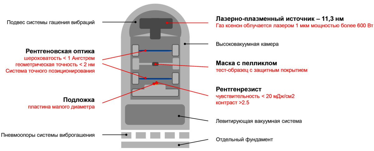
According to the article, this demo litho machine exists from 2011 and was planned to become eligible for industrial usage in 2013-2015. Considering that it is still in the demo stage, then probably the transition from the demo to production is very hard. Because otherwise, I wonder why is it still in the demo stage? Even the 30 nm use-case (which is mentioned in the 2011 readout) would already be a huge boon.Russia has created a prototype of a lithography machine that can do 7nm:


- Status
- Not open for further replies.
