Chinese semiconductor industry

Status
Not open for further replies.

gelgoog

Lieutenant General
Registered Member
8-inch should make this one of the largest production facilities for MEMS in the world I think. Those fabs typically use older tools and processes. MEMS are useful for making things like accelerometers and gyroscopes used in smartphones for example. These are usually fairly small in die area anyway.

With regards to SMEE, I think other than the commercial lithography machines they sell for packaging, the front-end lithography machines they developed are basically targeted at meeting the needs of Project 02 and the government's requirements. These machines are likely used to make military chips and other chips for the government in facilities we do not even know about. Given that the military requires mostly older chips with limited production runs, the capacity of the tools is sufficient. But there definitively needs to be a focus on making machines competitive for sale to commercial sites. The government needs to fund this effort, and I think SMEE needs to be radically expanded in size, it needs multiple teams working on multiple projects to plug all the gaps. There should be replacements for all lithography machines.

The other tool vendors need to do their own production and replace all imports of components they have as much as possible. And the whole tools industry will likely need to consolidate into just a couple major players. There are just too many companies and there is a lack of integrated tool chain. China needs to have like two companies similar to TEL. And there definitively is a need for another lithography company, even if it working on marginal developments like e-beam lithography or something like it.

I think the most likely way to do this would be to aggregate most of the other tools vendors into two large companies which would be centered around AMEC and Naura. Those would be beefed up to compete with TEL and Applied Materials. Lithography would remain separate.
 
Last edited:

paiemon

Junior Member
Registered Member
If I had to guess. They are already testing out with ICRD/SMIC/YMTC for a while and they are making adjustment and fixes. However, it probably isn't a good idea to start producing DUVi scanners before they have been verified to work in production settings at a profitable work load. Each customer have their own process and can probably provide SMEE with valuable feedback. Let's just say that if SMIC can put SMEE into their production process by early 2024 (like high volume regular production), then this would be pretty good.

Keep in mind that SSA600 was certified in 2018 and was only reported to be in production this year (so took 4 years). If SSA800 (which was certified last year) can be used in production process by early 2024, then that would be just 2 to 3 years.

In some ways, I think Huawei will have a leg up here if they have their own fab and their own lithography machine. They can just work with each other to fine tune the process. And Huawei likely does not care if the WPH is a little lower, since they have no other avenue to get their chips.
I agree that under normal scenarios it would be best to have an initial risk-production run using the SMEE tools, I was thinking under the current circumstances, they would take the risk and just put them straight into production use and subsidize the costs/drawbacks to the FABs just to get them into that feedback loop. On the other hand, the fact that they are willing to take the time to introduce it more gradually probably means that for projected operations at the fabs, lithography machines are not a limiting factor (whether through current stock, planned deliveries, future projections from ASML) which is a good thing. It could also mean that existing production floorspace is filled up to the point where a new dedicated line would have to be set up to accommodate SMEE equipment which could drag out the deployment which supports that the FABs are running flat out.
 

tokenanalyst

Brigadier
Registered Member
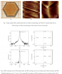
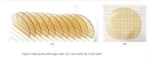
The 46th Research Institute of China Electronics Technology Group Corporation (referred to as the 46th Research Institute of CETC) has made important breakthroughs in the cultivation of high-quality AlN seed crystals, dynamic control of heat and mass transfer, and long-term stable growth. The crystal quality of the AlN single crystal has been greatly improved. At present, the 46th Institute of CETC can stably prepare 1-inch and 2-inch high-quality AlN single crystal substrates, and is also actively exploring the growth process of larger-sized single crystals.
Aluminum nitride (AlN), one of the typical representatives of ultra-wide bandgap semiconductor materials, is an ideal substrate material for a new generation of high-performance microwave power devices and ultraviolet optoelectronic devices. in,AlN single crystal substrates and related devices are research hotspots in the field of scientific research.
The AlN crystal structure is a hexagonal wurtzite structure with strong anisotropy. During the PVT growth process, the surface energy and growth rate of different orientation growth surfaces are very different. The high- quality AlN crystal profile prepared under ideal process conditions usually consists of (00±1) plane, (10n) plane and (100) plane, etc. Surrounded by several low-index crystal planes, the crystal head is in the shape of a regular hexagonal truss. There is also no "cellular structure" inside the crystal.

1672172525970.png1672172561579.png
 

FairAndUnbiased

Brigadier
Registered Member
8-inch should make this one of the largest production facilities for MEMS in the world I think. Those fabs typically use older tools and processes. MEMS are useful for making things like accelerometers and gyroscopes used in smartphones for example. These are usually fairly small in die area anyway.

With regards to SMEE, I think other than the commercial lithography machines they sell for packaging, the front-end lithography machines they developed are basically targeted at meeting the needs of Project 02 and the government's requirements. These machines are likely used to make military chips and other chips for the government in facilities we do not even know about. Given that the military requires mostly older chips with limited production runs, the capacity of the tools is sufficient. But there definitively needs to be a focus on making machines competitive for sale to commercial sites. The government needs to fund this effort, and I think SMEE needs to be radically expanded in size, it needs multiple teams working on multiple projects to plug all the gaps. There should be replacements for all lithography machines.

The other tool vendors need to do their own production and replace all imports of components they have as much as possible. And the whole tools industry will likely need to consolidate into just a couple major players. There are just too many companies and there is a lack of integrated tool chain. China needs to have like two companies similar to TEL. And there definitively is a need for another lithography company, even if it working on marginal developments like e-beam lithography or something like it.

I think the most likely way to do this would be to aggregate most of the other tools vendors into two large companies which would be centered around AMEC and Naura. Those would be beefed up to compete with TEL and Applied Materials. Lithography would remain separate.
I think AMEC isn't strong enough to be a core of a conglomerate. Their product diversity is low, but a large conglomerate needs experience in managing high product diversity, and worse, their product line somewhat overlaps with NAURA. Their revenue isn't even 5 billion RMB, making them too small to buy out other competitors with comparable revenue.

I think NAURA will definitely become a conglomerate like TEL or Applied Materials, but even in the US it's not just AMAT LAM KLA. They also have moderate or specialized companies like Onto Innovation, Axcelis, Veeco etc which serve niche markets and are about the same size as AMEC.

Instead I think we're going to see:

1 big conglomerate that does everything or sever high risk big projects, probably CETC

1 conglomerate in "chemistry" (etch/deposition/clean/develop), probably NAURA.

1 conglomerate in metrology and something tangentially related like maskless lithography, ebeam lithography or ion implantation (probably Dongfang Jingyuan, and probably in ebeam lithography)

1 conglomerate in standard projection lithography

A grouping of smaller specialized companies selling either top class equipment in 1 category or niche equipment in many categories.
 

tokenanalyst

Brigadier
Registered Member
I think AMEC isn't strong enough to be a core of a conglomerate.
They are getting closer to Piotech, maybe they are looking to expand their deposition offerings.

Increasing cooperation between Chinese semiconductor equipment manufacturers.

Tuojing Technology(sypiotech): Domestic replacement not only needs to ensure quality and reliability, but also needs to keep up with customers to develop new technologies​


Lv Guangquan, chairman of Tuojing Technology, pointed out that this general meeting of shareholders includes three proposals. The first proposal is to increase the quota for daily connected transactions in 2022, mainly including cooperation with China Micro Semiconductor Equipment Shanghai Co., Ltd. (hereinafter referred to as China Micro Company) (AMEC) , Shenyang Fuchuang Precision Equipment Co., Ltd. (hereinafter referred to as Fuchuang Precision) and Shenyang Scientific Instrument Co., Ltd. (RSIC semiconductor) of the Chinese Academy of Sciences (hereinafter referred to as Zhongke Instrument).


After the meeting, Lu Guangquan discussed the company's development and industry status with representatives of Aiji Micro's shareholders. He said that although domestic chip factories are currently undergoing large-scale expansion, the domestic production rate of equipment is still low. Under the wave of domestic substitution, local semiconductor equipment companies need to do a good job in two aspects, one is to improve the quality and reliability of their products, and at the same time to provide better services. The second is to develop new technologies and keep up with the pace of customers while participating in domestic substitution of mature products.

Regarding the proposal to increase the quota for daily related-party transactions in 2022, Zhao Xi, the secretary of the board of Tuojing Technology, pointed out that previously, the company reviewed and approved the "Proposal on Predicting the Company's Daily Related-party Transactions in 2022" at the 2021 Annual General Meeting of Shareholders. The annual amount of related party transactions is RMB 51.5 million. According to the needs of the company's business development and production and operation, the estimated amount of daily connected transactions in 2022 is increased by 69.5 million yuan. After the adjustment of the related party transaction quota, the daily related party transactions of the company in 2022 are expected to be no more than 121 million yuan.

Regarding the adjustment of the transaction quota of the three related parties, Zhongwei Company (AMEC) increased from the original 3.5 million yuan to 5.5 million yuan, Fuchuang Precision increased from the original 40 million yuan to 100 million yuan, and Zhongke Yi increased from 7.5 million yuan to 15 million yuan. Zhao Xi told Aijiwei that the company's specific related party transactions are mainly divided into two parts, one part is the purchase of raw materials or accepting labor services from related parties in the company's daily operations; the other part is to sell products to related parties.

Among the three related parties, Zhongwei Company directly holds 8.40% of the shares of Tuojing Technology Company, and Yin Zhiyao, chairman and general manager of Zhongwei Company, serves as a director of Tuojing Technology Company. In addition to direct investment, the two companies' day-to-day connected transactions also bring synergies to each other.

Previously, when Aijiwei communicated with Dr. Yin Zhiyao, chairman of the company at the general meeting of the company's shareholders, he pointed out that investing in Tuojing Technology Co., Ltd. is conducive to the three-dimensional development strategy of the company and the expansion of its business layout. Today, Lv Guangquan, chairman of Tuojing Technology, also pointed out that the company and China Micro Co., Ltd. cooperate in many aspects in film processing, and there are shared customers and shared suppliers, which can form a synergistic effect to a certain extent.

Talking about the company's development, Lu Guangquan told Aijiwei that the company's revenue in the first half of the year increased by 365% year-on-year, which was mainly due to two aspects: First, technological breakthroughs. In the first half of the year, the company's SACVD and ALD processes at 28nm and below New products have achieved results; second, a large number of shipments of traditional PECVD products have contributed to revenue growth.

In addition to business growth, Tuojing Technology also announced that it will invest 270 million yuan in Shanghai Lingang area to build a semiconductor equipment project, and is committed to quickly forming production and research and development capabilities, and to carry out research and development and industrialization of ALD. Lv Guangquan said that the Lingang subsidiary provides services to customers nearby, and provides production and technical support in concentrated areas. In addition, since new breakthroughs in the field also require continuous introduction of talents, it is more convenient for the subsidiary to register in Shanghai to attract talents.

Please, Log in or Register to view URLs content!
 

tonyget

Senior Member
Registered Member
Please, Log in or Register to view URLs content!

Sam CNS secures YMTC and SMIC as new customers in China this year

Sam CNS, a Korean semiconductor parts maker, is accelerating its advance into the Chinese market. This year, it succeeded in supplying products to major Chinese NAND flash and foundry companies, and is known to be seeking additional customers.

According to the industry on the 26th, Sam CNS has secured major Chinese semiconductor companies such as YMTC and SMIC as new customers.

Sam CNS is a ceramic STF (Space Transformer) specialist for probe cards. The probe card is a post-processing component that inspects the electrical performance of semiconductors, and sends electrical signals to the wafer to determine whether or not it is defective. The ceramic STF is a kind of substrate used to support the MEMS (Microelectromechanical System) pins that exchange electrical signals with the wafer within the probe card.

Ceramic STF is usually composed of dozens of layers and has a total of more than 1 million fine via holes (holes for electrically connecting layers to layers). If even one of these holes is defective, the entire product is judged to be defective, so product development is very difficult.

Sam C&S is the only company in Korea that possesses the entire process from the material of ceramic STF to commercialization with its own technology. Based on this technology, Sam CNS has secured various global semiconductor manufacturers as customers. Domestic Samsung Electronics and SK Hynix and overseas Intel, Micron and Kioxia are typical examples.


This year, it succeeded in expanding its market territory to Greater China. As a probe card company, which receives ceramic STF from Sam CNS, entered China's YMTC and SMIC as a new vendor, Sam CNS also entered into a deal. YMTC and SMIC are China's largest NAND flash and foundry companies, respectively. However, as it is in the early stages of entering the market, supply is not yet high.

It is also known that Sam C&S is seeking to secure new Chinese customers. An official from Sam CNS said, "Starting from this year, we started supplying products to major Chinese semiconductor companies in earnest, and it is possible to secure additional customers."

Meanwhile, Sam CNS is also focusing on product diversification. Currently, SAM CNS mainly produces ceramic STF for NAND flash, which is a type of memory semiconductor. As of the third quarter of this year, the proportion of the product in total sales is over 97%. Accordingly, Sam CNS developed a ceramic STF for DRAM and began supplying it from 2020, and is currently developing a ceramic STF for CIS (CMOS Image Sensor) and is conducting tests with major customers.
 

tphuang

Lieutenant General
Staff member
Super Moderator
VIP Professional
Registered Member
I agree that under normal scenarios it would be best to have an initial risk-production run using the SMEE tools, I was thinking under the current circumstances, they would take the risk and just put them straight into production use and subsidize the costs/drawbacks to the FABs just to get them into that feedback loop. On the other hand, the fact that they are willing to take the time to introduce it more gradually probably means that for projected operations at the fabs, lithography machines are not a limiting factor (whether through current stock, planned deliveries, future projections from ASML) which is a good thing. It could also mean that existing production floorspace is filled up to the point where a new dedicated line would have to be set up to accommodate SMEE equipment which could drag out the deployment which supports that the FABs are running flat out.

So I would love to hear input from others (@tokenanalyst @olalavn @PopularScience ). To the best my knowledge, the only chip makers that need DUV immersion scanners are
SMIC
HLMC
Huawei
CXMT
YMTC

CXMT and YMTC right now are stuck on expansion due to US sanctions. They probably have enough ASML scanners for near/medium term expansion plans Not limited by lithography machines, but limited by the progress of whoever is replacing KLA domestically.

HLMC's fab 6 is the only that requires DUVi scanners, but it's basically at capacity right now. A new fab has been speculated, but yet to be announced. Since a new plant is most likely 3 years away, I see no issue here. Things would have to be really crazy for SMEE scanners not to be ready by then.

Huawei's fab hasn't started production. Aside from ICRD, its foundry is likely the most dedicated at building an all domestic production line. As such, I think they will only start production once they are comfortable with their process. It's unlikely they will need that much capacity anyhow, so I don't think they will be bothered by longer time to put SMEE scanners in production. In fact, they might prefer it, since they will want to perfect their process first. They also are probably looking to build their own lithography machines.

Which brings us to SMIC. This is the question mark. We know they have a huge demand for ASML machines with the SMSC plants and also Beijing Capital and Lingang plants. We've also know they have been buying up a lot of ASML scanners recently (most likely to stock up). They will most likely only use ASML scanners for the advanced process at SN1 and SN2. I wouldn't be surprised if they are testing out their own process with SMEE scanner in their research facility or SMIC Capital plant. The question is if they will have enough ASML scanners to not suffer any interruption in their SMIC Capital and Lingang plant. I think it is likely they do (depending on how it goes with Dutch gov't). There is a chance they may be forced to slow down expansion if Dutch gov't imposes a strict sanction without any grace period and SMEE progress is slower than expected. That's the primary concern here. But if SMEE machines can actually be verified with production process and start mass production by Q3 and delivered before end of the year, I think the risks will be minimal.
 

PopularScience

Junior Member
Registered Member
What was the original expected timeline for them? It would be weird for me if dry machine is not already in mass production, since it was announced in that article about Shanghai's ic sector achievements. And we have seen them winning bids for it.


That's fine. I think there is a lot of value when they can get production ramped up for dry arf machines for local needs. I have also been pretty clear that I think it will take some time for them to ramp up production on arf immersion scanner. That's why they still need to buy and stock up large number of asml scanners. but it would be disappointing if they have not produced a small number of ssa800 for fabs to test with and debug the system. I am operating under the assumption that several Chinese fabs do have ssa800 for testing out process.


Sure, given their other struggles, I would say they are not the obvious choice here for euv. These are all large scale collaboration effort. All the advancement in duvi production is not going to help them much in advanced process if they don't have euvs in 5 years.
I remember original timeline was to deliver DUVi in beginning of this year.

ICRD Linggang just finished construction and moving in. Dry machine will be verified in ICRD Linggang production line before immersion machine. I expect mass production in second quarter.
 

PopularScience

Junior Member
Registered Member
Does this mean they are waiting for systems to be deployed and operational at SMIC/YMTC/Etc before proceeding to mass production. What does this mean for the testing that was taking place at ICRD for the final test units?
Before this it was verified in ICRD ZhangJiang, a small testing line. Now they will test/verify it in ICRD LingGang, a new fab with 2 actual production lines.
 
Status
Not open for further replies.
Top