The entry ceremony of Ruishi Chuangxin's first lithography machine was held in Liangjiang New District
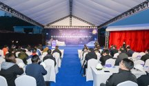
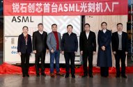
On December 27, the entry ceremony of the first lithography machine of the first phase of the Ruishi Chuangxin filter production base project was held in Shuitu New City, Liangjiang New District, marking the basic completion of the first phase of the project’s filter chip production base and officially entering the equipment Debugging phase.

Zhang Hongxing, member of the Standing Committee of the Municipal Party Committee and Secretary of the Party Working Committee of Liangjiang New Area, attended the event.
Yang Zhenghua, member of the party group and deputy director of the Municipal Economic Information Commission, Li Jie, member of the Party Working Committee and deputy director of the Management Committee of Liangjiang New Area, Li Jin, secretary of the party committee and chairman of Liangjiang Investment Group, and Ni Jianxing, chairman and general manager of Ruishi Chuangxin, attended the meeting. Xie Jing, general manager of Liangjiang Merchants Group, presided over the event.

It is reported that Ruishi Chuangxin is a company that focuses on the R&D and sales of high-performance 4G/5G RF front-end products. Its products have industry-leading performance and quality, and are mainly used in smartphones, Internet of Things terminals, and tablet computers.
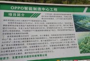
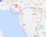
Located in Liangjiang New District, the new project (Phase I) of Ruishi Chuangxin MEMS device production base covers a total area of 120 mu, with a total investment of 2.2 billion. It will build a 4G/5G MEMS filter chip production base and a packaging and testing production base. Greatly improve the overall strength of Liangjiang New Area and Chongqing in the field of integrated circuit design and manufacturing.
Li Jie said in his speech that the cooperation between Ruishi Chuangxin and Liangjiang New Area has entered a new stage. He hoped that Ruishi Chuangxin will firmly cultivate Liangjiang and become bigger and stronger, so as to drive more industrial chain partners to settle in Liangjiang New Area. Liangjiang New District will lay a solid foundation for the development of the electronic information industry, focus on key areas such as integrated circuit design, manufacturing, packaging and testing, give full play to the advantages of leading enterprises, and strive to extend the chain and strengthen the chain. At the same time, continue to do a good job in corporate services, thoroughly implement the working mechanism for leading cadres to contact key enterprises, actively serve and serve first, actively coordinate and solve the development problems faced by enterprises, boost the confidence of enterprises in development, and create "no trouble, no need Bing" first-class business environment.
Ni Jianxing said in his speech that Ruishi Chuangxin, as the backbone of the localization of the semiconductor industry, especially the RF industry, has always taken technological innovation as its foundation, worked hard and made breakthroughs, and constantly made up for the shortcomings of the localization of the RF front-end. The establishment of Ruishi Chuangxin Chongqing filter factory has laid a key step for the breakthrough of domestic advanced discrete filter products and high-end filter modules. The smooth entry of lithography machines will provide a strong guarantee for the development and production quality control of Ruishi Chuangxin products, which will help further enhance the core competitiveness of Ruishi Chuangxin products, and is of great significance for improving the company's sustainable development capabilities.
At present, Chongqing is speeding up the construction of the whole industrial chain of "core screen devices and nuclear network" and the whole element group of "cloud-connected computing and computing" to create an electronic information industry cluster with international competitiveness. Liangjiang New District, as the main battlefield and important growth pole of Chongqing's economic development, is following the unified deployment of the municipal party committee and the municipal government, putting the high-quality development of the manufacturing industry in a more prominent position, empowering industrial development with technological innovation, and striving to build a modern industrial system achieve new breakthroughs.
Ruishi Chuangxin's 4G/5G MEMS filter and packaging and testing project, as the first RF front-end chip and module production and packaging and testing base for smartphones in Southwest China, will fill the gap in filter manufacturing in Chongqing, which is important for Chongqing's national integration It is of great significance to seize the opportunity in the field of circuit characteristic manufacturing technology and realize the domestic substitution of communication technology and big data intelligent innovation technology.
Relevant persons in charge of the Municipal Economic and Information Commission, relevant units in Liangjiang New Area and persons in charge of Ruishi Chuangxin participated.
