Chinese semiconductor industry

Status
Not open for further replies.

european_guy

Junior Member
Registered Member

Applied Materials: Chinese chip companies will adjust their process node strategies​


Please, Log in or Register to view URLs content!

"We anticipate that some customers may decide to change their plans or technology, so it will not exceed the threshold affected by the rule at this time," said Applied Materials chief financial officer Brice Hill.

"However, development of such process nodes and validation/qualification by customers will take some time,<...> as a result, Applied expects that companies in China with 14nm designs will continue to use that node and the services that the foundries can provide. Meanwhile, a hypothetical 17nm node (assuming it makes financial sense) could be used for an entirely different design. "

"Applied Materials said U.S. sanctions on China's semiconductor industry, which prevent it from supplying advanced equipment to Chinese customers, will cost it $2.5 billion in revenue in fiscal 2023, or 10% of its 2022 revenue."

I translate like: we are asking our customers, in a deperate attempt, to increase minimum rules from 14nm to 17nm, but we also understand this makes little sense (invest time and resource to take advantage of a possibly short-lived loophole that can be closed at any time), and so we expect to lose it all ($2.5 billion is far more than just advanced nodes in China).

IMO Applied Materials gave up on China market. They understand it's game over for them in China. They just don't want to admit it officially.

BTW "companies in China with 14nm designs will continue to use that node" it's very telling, it means customers will use alternative equipment for 14nm.
 

tphuang

Lieutenant General
Staff member
Super Moderator
VIP Professional
Registered Member
That's odd,why would SMIC needs to assuring their US customers that SMIC meets regulations?Because the US regulation is all about selling to Chinese fabs,not buying from Chinese fabs. US entities can buy 3nm chips from SMIC if SMIC can make it,and it's totally legit under current US regulation.
They need to assure customers that there are no more Americans working at SMIC and that they are not using any 16nm and below tools provided by American firms.

See below, only 17nm is possible and that's if SMIC signs an agreement that none of its production will end up in Chinese military.

Applied Materials: Chinese chip companies will adjust their process node strategies​


Please, Log in or Register to view URLs content!

"We anticipate that some customers may decide to change their plans or technology, so it will not exceed the threshold affected by the rule at this time," said Applied Materials chief financial officer Brice Hill.

"However, development of such process nodes and validation/qualification by customers will take some time,<...> as a result, Applied expects that companies in China with 14nm designs will continue to use that node and the services that the foundries can provide. Meanwhile, a hypothetical 17nm node (assuming it makes financial sense) could be used for an entirely different design. "

"Applied Materials said U.S. sanctions on China's semiconductor industry, which prevent it from supplying advanced equipment to Chinese customers, will cost it $2.5 billion in revenue in fiscal 2023, or 10% of its 2022 revenue."

I translate like: we are asking our customers, in a deperate attempt, to increase minimum rules from 14nm to 17nm, but we also understand this makes little sense (invest time and resource to take advantage of a possibly short-lived loophole that can be closed at any time), and so we expect to lose it all ($2.5 billion is far more than just advanced nodes in China).

IMO Applied Materials gave up on China market. They understand it's game over for them in China. They just don't want to admit it officially.

BTW "companies in China with 14nm designs will continue to use that node" it's very telling, it means customers will use alternative equipment for 14nm.
Yeah, the entire idea that Chinese companies will adjust their strategies by doing 17nm node just so that they can buy AMAT tools is kind of ridiculous. And when he is talking about Chinese customers, he is just referring to SMIC here. No one else is really producing 14nm nodes right now.

Please, Log in or Register to view URLs content!
China’s imports of IC manufacturing equipment decrease by 16% year on year in quantity and increase by 6.5% in value in October
this says it all. Importing less equipment but more expensive ones (26% more expensive vs a year ago). The mature nodes are being increasingly supplied by domestic tools makers. Higher value simply means they are actually importing more not less advanced node tools.

I'd love to hear other's take on this, but it tells me they are increasing equipment expenditure on ASML machines. Given that American companies were cut off in October, it's unclear to me which other non-American firm they could've spent large amount of money on and gotten their deliveries in such a short time.
 

theorlonator

Junior Member
Registered Member
They need to assure customers that there are no more Americans working at SMIC and that they are not using any 16nm and below tools provided by American firms.

See below, only 17nm is possible and that's if SMIC signs an agreement that none of its production will end up in Chinese military.

Yeah, the entire idea that Chinese companies will adjust their strategies by doing 17nm node just so that they can buy AMAT tools is kind of ridiculous. And when he is talking about Chinese customers, he is just referring to SMIC here. No one else is really producing 14nm nodes right now.

Please, Log in or Register to view URLs content!

this says it all. Importing less equipment but more expensive ones (26% more expensive vs a year ago). The mature nodes are being increasingly supplied by domestic tools makers. Higher value simply means they are actually importing more not less advanced node tools.

I'd love to hear other's take on this, but it tells me they are increasing equipment expenditure on ASML machines. Given that American companies were cut off in October, it's unclear to me which other non-American firm they could've spent large amount of money on and gotten their deliveries in such a short time.
Probably Tokyo Electron, hopefully more Nikon too.
 

tphuang

Lieutenant General
Staff member
Super Moderator
VIP Professional
Registered Member
Probably Tokyo Electron, hopefully more Nikon too.
Were they ordering large amount of Nikon or tel equipment before this? I agree that after the news came out, Japanese tool makers likely won quite a few orders, but I am not sure they would have been delivered so soon.

@tokenanalyst you would know better than most here. What other non American tool makers were winning a lot of bids earlier this year that could have delivered in October to make up for the drop in American tools? I am really quite surprised that their import value is up for October.
 
Last edited:

hans_r

New Member
Registered Member
Were they ordering large amount of Nikon or tel equipment before this? I agree that after the news came out, Japanese tool makers likely won quite a few orders, but I am not sure they would have been delivered so soon.

@tokenanalyst you would know better than most here. What other non American tool makers were winning a lot of bids earlier this year that could have delivered in October to make up for the drop in American tools? I am really quite surprised that their import value is up for October.
The order was most certainly of ASML scanners - Japan's trade statistics show a decline of 17% by quantity, increase of 6% by value of semiconductor machinery exports to China.
Please, Log in or Register to view URLs content!

United States October 2022 trade data won't come out until December 6, 2022 and I'm not sure how to navigate Eurostat's website for trade statistics
 

tokenanalyst

Brigadier
Registered Member

In order to avoid regulatory risks, some brand manufacturers check the panel supply chain in advance​


Jiwei.com news, according to the Economic Daily, TrendForce said a few days ago that in order to prevent the further expansion of the US ban on China to the panel field, some brand manufacturers have recently begun to check the semiconductor-related supply sources of the panel supply chain and carry out countermeasures in advance.

TrendForce expects that with the development of semiconductor control regulations, the panel driver IC supply chain may gradually diverge, and develop towards the two extremes of "de-beautification" and "de-centralization". Although there is no problem of banning the panel for the time being, it is possible that the selection of driver ICs, wafer foundries, and packaging and testing plants will start to diverge. The test factory is required not to use the relevant semiconductors supplied by manufacturers in mainland China.

The United States promulgated new regulations to prohibit the export of advanced semiconductors and related manufacturing equipment involving U.S.-developed technology to mainland China. It is speculated that if the conflict spreads to display panels, the United States may take two measures to prevent panel production in mainland China. One is to ban the U.S. Universal The phosphorescent OLED materials produced by Display (UDC) are exported to China, and the second is to prohibit manufacturers in mainland China from using glass substrates produced by Corning Corporation of the United States.
 

tokenanalyst

Brigadier
Registered Member

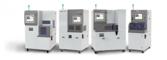
Han's Laser: The SiC ingot laser slicer applied to the third-generation semiconductor is being verified with customers​


575725890367.02341550690841882.5786.jpg


Jiwei.com news (text/Bai Yuxuan) On November 21, Han’s Laser said on the investor interaction platform that “laser cold cutting has shown great advantages in the field of silicon carbide cutting, and Infineon has also laid out this area. Does your company have any research and development reserves or products in this area?" and other inquiries said that the SiC ingot laser slicer used in the third-generation semiconductor is being verified with customers.

In addition, in terms of the photovoltaic sector, Han's Laser has continued to increase investment in research and development. By introducing a core talent team, Han's Laser has already possessed the R&D and manufacturing capabilities of the battery segment tube vacuum main equipment. The company has a complete product layout in the TOPCON field, and gradually has the R&D and manufacturing capabilities of the entire TOPCON battery industry chain equipment; in the HJT battery, it has deployed PECVD, PVD and other equipment products. The company's existing research and development projects include low-pressure boron diffusion furnace, Topcon laser boron doping equipment, LPCVD equipment, etc., and the low-pressure boron diffusion furnace and Topcon laser boron doping equipment are in the customer verification stage.

Please, Log in or Register to view URLs content!
 

tokenanalyst

Brigadier
Registered Member

Akeris, a semiconductor equipment manufacturer, completed tens of millions of strategic financing.​


At present, Akiris aims at the semiconductor packaging market, and has developed a series of 6-12 inch grinding wheel dicing machines against the leading imported models in the industry. The grinding wheel dicing machine is essentially the application of ultra-thin diamond grinding wheel ultra-precision cutting and grinding technology in the semiconductor packaging process. It has shown obvious competitiveness in terms of precision, production efficiency, and cost performance. It has been successfully applied in batches by leading companies in subdivided fields such as lithium tantalate, Mini LED, ceramic packaging substrates, magnetic devices, and power devices.

1669049027735.png

"Looking at the semiconductor processing process, from the ingot to the single chip, ultra-precision grinding technology is used in wafer ingot rounding, substrate chamfering, thinning polishing, CMP polishing, back thinning, wafer dicing, post-packaging cutting, etc. The process has a wide range of applications. Unfortunately, most of these technologies and equipment rely on imports. In the future, Akeris will be deeply involved in the semiconductor field, and will continue to keep customers competitive in line with customer needs and driven by technological innovation. Based on the concept of force, the ultra-precision grinding technology learned by the team at the National High-Efficiency Grinding Engineering Center of Hunan University is applied to the semiconductor field to provide a completely independent and controllable ultra-precision grinding overall solution. After completing this round of financing, we will Continue to optimize and iterate the dicing machine product line, and make technical reserves for new projects."

"Under the trend of domestic substitution of dicing machines, Akeris independently developed the key components of dicing machines, accumulated dozens of material scribing processes, and provided equipment, process design, material selection and generation for pan-semiconductor and semiconductor customers. Diversified services such as processing. The first acquaintance with Akeris stems from the team's enthusiasm, pragmatism and persistence in entrepreneurship. I believe that after landing in Hefei, the company will be able to closely integrate with Hefei's integrated circuit related industry chain and create more beautiful sparks. "

Please, Log in or Register to view URLs content!
 
Status
Not open for further replies.
Top