Chinese semiconductor industry

Status
Not open for further replies.

ansy1968

Brigadier
Registered Member
The chip market is giving signs it is heading towards a serious glut: Intel's news of laying 20k personnel is a serious indicative of this glut. China is increasing its manufacturing capacities, rightly so, because it is replacing imported chips. China can increase considerably its manufacturing capacity without running of of market for those chips. It simply substitutes foreign made chips.

What on earth is TSMC doing building new factories in US and thinking of building new factories in EU and Japan.

Are they stupid?
Bro to add on your post from Tom's Hardware.

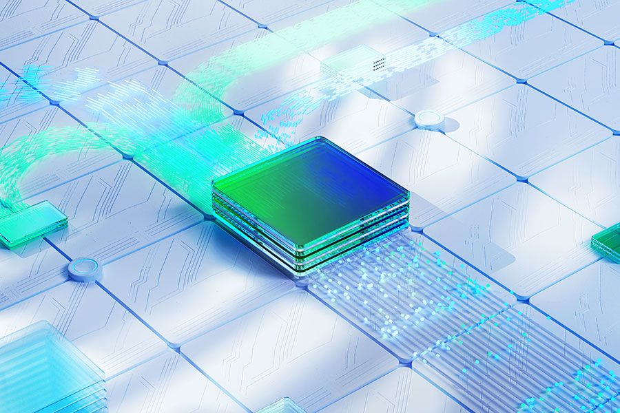
Apple's Chip Purchase from Arizona Might Be Marketing Trick: Report​

By
Please, Log in or Register to view URLs content!

published about 1 hour ago
Apple's dependence on Taiwanese chips will hardly end any time soon.
Apple M1 Max

(Image credit: Apple)

While Apple is expected to buy chips from
Please, Log in or Register to view URLs content!
in Arizona in a bid to lower its reliance on manufacturing in Asia in general, it does not look like the company will ever truly rely itself from Taiwanese chipmaking. As such, our colleagues from
Please, Log in or Register to view URLs content!
believe that the
Please, Log in or Register to view URLs content!
, which yet has to be officially announced, is more of a marketing gimmick rather than a decision based on necessity.

But while Apple is yet to confirm the plan to use TSMC's fab in Arizona, which is set to come online in 2024, let us analyze what Apple might need two years from now and what TSMC is going to offer the mighty company in a couple of years. What you have to bear in mind is that we know about Apple's supposed intention to use the fab in Arizona only from a
Please, Log in or Register to view URLs content!
report. We assume that the information is accurate as Bloomberg is very reputable source, but we cannot verify it.

Apple's Needs​

TSMC's fab in Arizona will produce chips using the company's N5 (5nm class) family of process technology, which includes N5, N5P, N4, N4P, and N4X. At present Apple uses N5, N5P, and N4 for various system-on-chips used for smartphones, PCs, and consumer electronics. Meanwhile, from reports, we know that Apple, being TSMC's alpha customer for leading-edge process technologies, is the first company to use TSMC's N3 (3nm class) node for at least one of its SoCs.


But designing chips for a leading-edge process technology (we are looking at a ~$600 million just for physical implementation and embedded software) and producing them on a leading-edge node is expensive. Apple uses its N4-based A16 Bionic SoC only for its premium iPhone 14 Pro, which sells from $999. Meanwhile, the more mainstream vanilla iPhone 14 (from $799) still uses the N5P-based A15 Bionic SoC from 2021.
Perhaps a more colorful example would be Nvidia's launch of its 4N (a customized version of N4 with significant performance enhancements) graphics processors based on the Ada Lovelace architecture. The AD102 and the AD103 GPUs are used exclusive for the company's flagship GeForce RTX 4090 and the RTX 4080 graphics boards that carry a $1,599 and a $1,199 price tags respectively (and these are the
Please, Log in or Register to view URLs content!
available today, so to speak). By contrast, AMD's range-topping Radeon RX 7900 XT and RX 7900 XTX (based on the Navi 31 GPU) use TSMC's N5 technology and will retail for $999, and $899, respectively, starting December 13.

But while the new process is expensive, Apple needs leading-edge production nodes not only for flagship smartphones, but also for its PCs. The company's M1-based Macs smashed some performance records and clearly exceeded expectations. Meanwhile, the Apple's M1 Max with its 57 billion transistors — one of the most complex chips ever designed — implemented on TSMC's N5P process demonstrates that the company's ambitions for performance are high to put it mildly.

TSMC's Capabilites​

While we think we know some vectors of Apple's SoC development, we need to analyze them in context with TSMC's plans and capabilities. And they, perhaps, will give some additional food for thoughts.
Back in October, TSMC cut its 2022 CapEx by $4 billion for the second time this year citing slowing demand for chips in the medium-term future as well as availability of wafer fab equipment (WFE). The reduced CapEx will not have an immediate effect on the company's business, but lowered spendings and prolonged lead time for fab tools could have an impact on TSMC over the next few years. In fact, WFE availability seems to be a major problem for the semiconductor industry in general.
TSMC's move to cut down its CapEx from $40 billion to $36 billion was a little bit surprising as the company's revenue and profits set all-time records in the third quarter of 2022. The company's earnings reached $20.33 billion, a 35.9% year-over-year increase and an 11.4% quarter-over-quarter increase. The company's net income in Q3 2022 totaled $8.717 billion, up from $4.849 billion in Q3 2021.
TSMC's main profitability driver these days is aggressive adoption of its advanced fabrication technologies, N7 and N5 (5 nm and 7 nm-class, respectively) by its customers in general and Apple — TSMC's largest client — in particular. In the third quarter TSMC's N5 family of production nodes became the largest revenue contributor as it accounted for 28% of the company's revenue (up from 18% in Q3 2021), which is not particularly surprising as the company ramped up production of multiple high-profile products from high-profile clients like Apple (M2, A16), AMD (Zen 4 CCDs), Nvidia (H100, AD102, AD103, AD104), and Qualcomm (Snapdragon 8+ Gen 1). Meanwhile, N7 manufacturing technologies (and Apple still uses it to male its A16 Bionic SoCs) accounted for 26% of TSMC's earnings (down from 34% in Q3 2021). As it turns out, 54% of the world's No.1 foundry revenue was contributed by its advanced nodes (up from 52% in Q3 2021).
Nonetheless, TSMC cut down its capital expenditure from $40 billion to $36 billion citing mid-term outlook and WFE availability, but not citing U.S. sanctions against Chinese supercomputer and semiconductor industries.
Indeed, demand for PCs and smartphones is dropping and some say that the bottom is yet to be reached. Meanwhile, high-performance computing products (i.e, a vague term that TSMC uses for products for PCs, HPC, and other performance-hungry applications) now account for 39% of TSMC's revenue, representing a slow yet stable growth. Meanwhile, as
Please, Log in or Register to view URLs content!
, HPC contribution to TSMC's revenue is also expected to decrease, which will reduce utilization of the foundry's N7 capacity to around 70% in Q4 2022 and 1H 2023, according to analysts from
Please, Log in or Register to view URLs content!
.

Slowing Down Capacity Expansion and How It Affects Macs​


Analysts believe that TSMC's CapEx reductions will slowdown capacity expansion for TSMC's N6/N7 production nodes, one the company's most important revenue contributors today. Meanwhile, since the foundry will have spare N7-capable capacities in the coming quarters, it will redeploy some of these production lines to make advanced chips on its N4/N5 nodes.
"TSMC will redeploy some N6/N7 idle capacity for N4/N5 and slow Fab 22 expansion (built for N7/N28)," wrote analyst Szeho Ng in a note to clients.
While the company said nothing about slowing down capacity expansion for N5 family of fabrication processes, it said that it expects N6/N7 demand to pick up in the second half of 2023, which is when utilization rates of N7-capable product lines increases.
Meanwhile, it is unclear how the CapEx cut will affect ramp up of the company's N3 (3 nm-class) family of fabrication technologies. And this is where it concerns Apple: we have no idea what it produces at N3. Apple may use N3 for its PC-bound processors. Those Macs may well not end up in in the popular things like Mac Mini, MBA, or MBP 13 Pro, but there are expensive Mac Studio and MacBook 14/16 machines that could absorb the cost. Yet the thing is, nobody knows what Apple plans to do. All we know is based on comments from the China Renaissance financial analyst firm which tends to be accurate, but it is not an official source.
"We expect 2023 CapEx to be flat," wrote the analyst. "We expect 2023 CapEx focus will be to get ready for future N4/N5 demand waves with Qualcomm/Nvidia planning moves from [Samsung Foundry]. The pace of TSMC's N3 buildout plans is more muted, behind N5/N7 expansion pace at similar stages of ramp-up given an initial concentrated clientele and cost concerns.

Summary​

While we do not know what exactly Apple plans with its future chips, we certainly know that the Arizona fab may not suffice its ambitious Apple Silicon plans. But will the company need chips produced there? Absolutely! Will it be a marketing gimmick? We can only wonder at this point.
 

gelgoog

Lieutenant General
Registered Member
Making the TSMC US fab with the 2nd best process, with expensive paid staff, who are not willing to work long hours, will make this factory not cost competitive. If it is used to make 2nd tier smartphone chips for low income nations like India even more of failure it will be. Samsung already has had an experience where they built a fab in the US with their best process back then even (14nm) and it was still a failure.
 

tokenanalyst

Brigadier
Registered Member

Study on Uniformity of Thin Films Prepared by Ion Beam Sputtering Deposition Equipment​


Chen Guoqin, Yuan Zuhao, Hu Fan, Fan Jianghua

(The 48th Research Institute of China Electronics Technology Group Corporation, Changsha, Hunan 410111)

Abstract: Aiming at the uniformity of the thin film of the ion beam sputtering deposition equipment, the method of combining theoretical analysis and calculation with experiments was used to calculate the distribution difference of the thin film thickness, and thus the shape of the correction plate was designed. Experimental results showed that the corrected film uniformity increased from 32% to 1.7%.

1668991510693.png1668991535923.png
1668991671689.png
Please, Log in or Register to view URLs content!
 

MortyandRick

Senior Member
Registered Member
Sure, see the images below.


No, it does not. The Statista article references the National Center for Education Statistics Digest of Education Statistics which reports degrees by field of study
Please, Log in or Register to view URLs content!
Biological and Biomedical Sciences: 126,590
Engineering: 128,332
Engineering Technologies: 19,788
Computer/Information Sciences: 91,752
Mathematics and Statistics: 27,216
Physical Sciences: 30,738
Adding these together gets you to 424,416 issued degrees


Health Professions: 257,282 degrees would put you way over
You just invalidated your own argument. There's a difference between health sciences and health professionals. Biological and biomedical sciences are part of health sciences, it never included health professionals. So yes it is lower of you exclude health sciences.
 

tokenanalyst

Brigadier
Registered Member

China speeds up research on key technologies of graphene​


Jiwei.com report (article/Li Ying) Recently, the 2022 (Ninth) China International Graphene Innovation Conference was held in Baoshan District. The theme of the conference is "Shanghai Polyolefin Power Co-Carbon New Future", focusing on industrial chain cooperation and deep integration of production, education, research and application.

1524941104213.0645.jpg


At the conference, the Graphene Copper Innovation Consortium was announced. It brings together Chint Group, Shanghai Electric Cable Institute and Shanghai Graphene Industry Technology Functional Platform, etc., and will "publish the list" for the world, jointly carry out key technology research, and focus on solving a number of "stuck neck" problems.

When the current silicon-based chip technology is gradually approaching the limit, China's semiconductor industry hopes to develop advanced graphene chip technology to replace silicon-based chips, so as to solve the problem of silicon-based performance limits. The performance of graphene chips will be 10 times higher than that of silicon-based chips, while the power consumption is much lower than that of silicon-based chips. The research and development of graphene chips may break the technological monopoly of the United States in the semiconductor field.

As China has concentrated its efforts in the field of graphene, breakthroughs have been made. By the end of 2021, China's graphene patent technology applications accounted for about 80% of the world's total, and the market size of related products has reached 16 billion yuan.

It is worth noting that the Ministry of Industry and Information Technology announced not long ago that it has recently approved the establishment of three national manufacturing innovation centers including the National Graphene Innovation Center. The Innovation Center will focus on the weak link in the development of the graphene industry, focus on the research and development directions of large-scale preparation of graphene materials, industrial application of graphene materials, and quality improvement of the graphene industry, and carry out key common technological breakthroughs to support the creation of an innovation chain that runs through the graphene field The innovation system of industry chain, capital chain, talent chain and value chain will boost the further innovation and development of the domestic graphene industry.

Please, Log in or Register to view URLs content!
 

tokenanalyst

Brigadier
Registered Member

Li Yang's research group from the Department of Precision Instruments achieved efficient preparation of lithium niobate microring cavities with a Q value of nearly 10 million based on wet etching.

Please, Log in or Register to view URLs content!

Tsinghua News Network, November 9th
Lithium niobate is a ferroelectric crystal with high electro-optic coefficient and second-order nonlinear coefficient, and is the core material of modern electro-optic devices. Lithium niobate thin film on insulator (TFLNOI) enables many devices based on the bulk material lithium niobate to be integrated on the chip, thereby greatly reducing the size of the device and improving the performance of the device. Among them, the micro-ring cavity is the core structure of on-chip lithium niobate electro-optic and nonlinear devices. The micro-ring cavity with higher quality factor allows the signal light to go around more circles in it, so as to achieve a stronger optical field and more effective electro-optic or Nonlinear Optical Transformation (Fig. 1). Combining the excellent photoelectric characteristics of lithium niobate and the high quality factor of TFLNOI microring/waveguide, high-performance electro-optic modulators, optical quantum information devices, nonlinear wavelength converters, optical frequency combs and other devices can be realized.
At present, the mainstream method to achieve large-scale and high-quality device processing on the TFLNOI platform is inductively coupled plasma-reactive ion etching (ICP-RIE). Although ICP-RIE can achieve microrings with an intrinsic quality factor higher than 10 million, it has limitations such as limited throughput and unstable process parameters. In addition, lithium is currently considered to be a polluting element in the CMOS process. The ICP-RIE equipment used for TFLNOI micro-nano processing requires "special materials and special materials", which cannot be compatible with the current CMOS process equipment, which increases the processing cost.

In response to the above challenges, the team of Associate Professor Li Yang from the Department of Precision Instruments, Tsinghua University conducted research on the wet etching process of TFLNOI (Figure 2). Based on a solution composed of ammonia and hydrogen peroxide, the team fabricated waveguides and microrings on x-cut and z-cut TFLNOI, respectively, and conducted a systematic study on the anisotropy of the solution for x-cut and z-cut TFLNOI etching (image 3). This wet etching process can not only achieve processing quality comparable to ICP-RIE, but also has unique advantages in process and device performance. The relevant results were published in Advanced Materials under the title of " High-Q thin film lithium niobate microrings fabricated with wet etching" ( High-Q thin film lithium niobate microrings fabricated with wet etching ) , And was selected as " Editor's Choice " (Editor's Choice).

1669003272963.png
 

tokenanalyst

Brigadier
Registered Member

Wuhan Yuwei Optics successfully developed OPC software for computational lithography​


Recently, Wuhan Yuwei Optics Software Co., Ltd. (hereinafter referred to as "Uwei Optics") has successfully developed a nationally produced, independently controllable computational lithography OPC software. Currently doing integration and testing, and going to the chip manufacturer for verification.

Yuwei Optics was established in October 2020. Relying on the important achievements made in the field of integrated circuit manufacturing for more than ten years by national-level platforms such as the State Key Laboratory of Digital Manufacturing Equipment and Technology of Huazhong University of Science and Technology and Wuhan Optoelectronics National Research Center, the company is committed to Independent development of photolithographic mask optimization design technology and software (OPC software).

In July this year, Yuwei Optics completed the A round of financing of tens of millions of yuan. After the completion of this round of financing, Yuwei Optics will further strengthen the integration and software productization of each core module, and at the same time calibrate, test and verify various software parameters.

Professor Liu Shiyuan said that before the lithography manufacturing of chips below 90nm or even 180nm, a type of algorithm software called OPC (Optical Proximity Correction) must be used for optimization. OPC is a type of EDA (Electronic Design Automation) industrial software. Without OPC, all IC manufacturers will lose the ability to convert chip designs into chip products.

China Optics Valley news shows that Professor Liu Shiyuan, the founder of Yuwei Optics, Huazhong University of Science and Technology, is the director of the Integrated Circuit Measurement Equipment Research Center of Huazhong University of Science and Technology, and also the director of the Integrated Circuit Measurement and Testing Technology Innovation Center of Optics Valley Laboratory. In 2002, he joined Shanghai Microelectronics Equipment Co., Ltd. (SMEE). It established SMEE's first control engineering laboratory, which solved the technical problems of synchronous control of mask table, workpiece table, and exposure dose in scanning projection lithography machines.

Please, Log in or Register to view URLs content!
 
Status
Not open for further replies.
Top