I hope that they succeed sooner rather than later.... DUV and EUV lithography is extremely difficult... In as much as one hopes for miracles and a sudden observation and identification of a missing step necessary to complete a process, this stuff ain't easy...I thought it would be good to summarize the present state of the Chinese lithography industry at this point of YOOL 2022:
DUV:
EUV:
- The SSA800 has met expectations (or disappointed them, depends who you ask) and delivered to customers for 28nm production. It is roughly comparable to an ASML NXT:1980Di. China has achieved completely indigenous 28nm volume production.
- The SSA800 is expected to be used in 14nm production through multipatterning next year.
- A follow-on DUVL machine (name unknown) using a more powerful light source and improved workbench for single exposure production of 22nm and multipatterning of 7nm (perhaps 5nm?) is expected Soon™. Expected to be comparable to ASML NXT:2050i.
I'd welcome the inputs, thoughts, and critiques of knowledgeable members like @WTAN, @tokenanalyst, and @FairAndUnbiased.
- There were some rumours of a 150W DPP EUVL tool supposed to be released around now. Obviously, no such thing has materialized, which means it's A) very secretive or B) as I suspect, DPP is not a viable path to commercial EUV.
- Everything about LPP EUV is a black box (at least in comparison to DUV). No word on the status of the CO2 laser, the optics, etc. All we "know" is that a machine should be ready around 2025.
- SSMB is a very interesting dark horse, but I don't think it's in the running for China's first generation EUVL. If it lives up to its promise, it would be a vast improvement over LPP EUVL and China would gain enormous advantages from getting to it first.
You are using an out of date browser. It may not display this or other websites correctly.
You should upgrade or use an alternative browser.
You should upgrade or use an alternative browser.
Chinese semiconductor industry
- Thread starter Hendrik_2000
- Start date
- Status
- Not open for further replies.
SMIC has already demonstrated a 7nm process, so the tools it has at its disposal should be sufficient to tide China over until SMEE/Huawei/CETC come out with their own tools. Chinese companies also demonstrated 10kW CO2 lasers a decade ago, so it's very reasonable to assume China has a 30kW laser today or will have one shortly. I'm quite sanguine about China's prospects in lithography and very hopeful in new fields like photonic chips, next-generation materials, quantum computing, etc. In anything where the West doesn't have a legacy advantage, it's going to lose badly.I hope that they succeed sooner rather than later.... DUV and EUV lithography is extremely difficult... In as much as one hopes for miracles and a sudden observation and identification of a missing step necessary to complete a process, this stuff ain't easy...
The problem with the US's sanctions is succinctly expressed by
escobar
Brigadier
In the long run, meanwhile, the U.S. may have given up what would have been, thanks to the sheer amount of cost and learning curve distance involved, a permanent economic advantage. Absent politics there simply is no reason to compete with TSMC or ASML or any of the other specialized parts of the supply chain; it would simply be easier to buy instead of build. Now, though, it is possible to envision a future where China undercuts U.S. companies in chips just like they once did in more labor-intensive industries
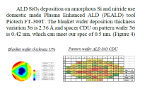
Another thing I didn't mentioned about this paper is that apart from Naura etching tools they are using Piotech deposition tools.They are in the process of validation.
View attachment 100332
A 5nm node has many layers, way too many, from the most critical to the less critical ones, they may use AMEC, lam research, TEL, Naura, CETC to even PNCS wet etching tanks for making those layers, in this case they are using Naura for the most critical ones.
That is the problem with this new sanctions for US companies, because a lot of tools are used between multiple nodes in different layers, even older tools there where not designed at first for below 7nm nodes.


Paul Triolo isn't Blob or Pundits but he's kind of sceptical of total indigenization
This isn't saying much. What are the specifics that can't be done and are physically impossible to occur? What makes a particular technology inherently non-Chinese and can never ever be replicated in China?Paul Triolo isn't Blob or Pundits but he's kind of sceptical of total indigenization
He seems to be referring to what would be true in normal economy where Chinese companies could just buy from ASML and Cadence as they saw fit, and thus have no economic reason to create local alternatives to this long list of highly specialized monopolies.This isn't saying much. What are the specifics that can't be done and are physically impossible to occur? What makes a particular technology inherently non-Chinese and can never ever be replicated in China?
I think he misjudges why say a special laser, that is only made in small numbers, is made only by a single firm. Is it because this firm has a number uniquely talented people and highly secret recipes? Or is it because there is simply isn’t enough market for a competitor? He seems to think the former but reality is clearly the latter.
Paul has also been insistent that the SMIC 7nm is no true 7nm (while seemingly missing that the chip was made in 2021 and not 2022).Paul Triolo isn't Blob or Pundits but he's kind of sceptical of total indigenization
- Status
- Not open for further replies.

