Chinese semiconductor industry

Status
Not open for further replies.

hvpc

Junior Member
Registered Member
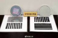
it seems that 22nm process rumors 2 years ago have appeared.... and 10nm process rumors have appeared
View attachment 100297
Could someone translate this? The only thing I recognize here (22nm@365nm) doesn't make sense at all.

Even if someone decided to create an immersion iLine scanner, the theoretical minimum half pitch would be ~68nm.
(assuming theoretical minimum k1 of 0.25, NA of 1.35, and wavelength 365nm).

I call B.S. if this piece is really claiming 365nm iLine system could generate 22nm feature size.
 
Last edited:

ansy1968

Brigadier
Registered Member
it seems that 22nm process rumors 2 years ago have appeared.... and 10nm process rumors have appeared
View attachment 100297
Sir use in Beidou system ;)

Please, Log in or Register to view URLs content!


Nov 24, 2020 — A more advanced chip is ready for the market. The chip will support dual-frequency positioning, which will further increase the accuracy of the ...
 

supersnoop

Major
Registered Member
Isn't that par for the course for this admin?

Do you guys remember:
1) Supposed investigation into Wuhan laboratory they made a huge deal of in 2021
2) Afghan withdraw
3) Transitory inflation
4) Blowing up Nordstream 2, effectively neutering Europe's industrial capabilities.
5) Miraculously managing to piss off Iran and Saudi Arabia simultaneously.

This really is par for the course though. They didn't even properly consult semiconductor experts in the U.S., let alone allied nations, before coming up with these sanctions. And they have the galls to call Trump stupid and immature.

Yeah they are investigating Seagate for selling hard drives to Huawei.

Really scraping the bottom of the barrel

Please, Log in or Register to view URLs content!

Next they will investigate American Standard for supplying toilets to Huawei.

Edit:
Oops, already posted
 

gelgoog

Lieutenant General
Registered Member
Could someone translate this? The only thing I recognize here (22nm@365nm) doesn't make sense at all.

Even if someone decided to create an immersion iLine scanner, the theoretical minimum half pitch would be ~68nm.
(assuming theoretical minimum k1 of 0.25, NA of 1.35, and wavelength 365nm).

I call B.S. if this piece is really claiming 365nm iLine system could generate 22nm feature size.
This machine uses multiple exposures. It will not be price competitive for mass production.
 

hvpc

Junior Member
Registered Member
This machine uses multiple exposures. It will not be price competitive for mass production.
Not according to the article (I found article that mentioned 22nm@365nm), it said it's 22nm in a single exposure.
Please, Log in or Register to view URLs content!


1666859148327.png

1666859203077.png

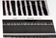
This bogus claim that 365nm wavelength could achieve 22nm resolution was laughed at by the industry a couple years ago. The definition used by these guys on what they considered to be good resolution (limit) is a joke. Just take a look at the very simple Line/Space pattern they showed.

You don't have to be a semiconductor lithography expert to see the proof these guy provided is not an 'acceptable resolution' to be taken seriously. The line edge roughness, CD uniformity, sidewall angle of these line/space that's supposed to be 1:1 ratio are just hideous.
 
Last edited:

tokenanalyst

Brigadier
Registered Member
Not according to the article (I found article that mentioned 22nm@365nm), it said it's 22nm in a single exposure.
Please, Log in or Register to view URLs content!


View attachment 100302

View attachment 100303

This bogus claim that 365nm wavelength could achieve 22nm resolution was laughed at by the industry a couple years ago. The definition used by these guys on what they considered to be good resolution (limit) is a joke. Just take a look at the very simple Line/Space pattern they showed.

You don't have to be a semiconductor lithography expert to see the proof these guy provided is not an 'acceptable resolution' to be taken seriously. The line edge roughness, CD uniformity, sidewall angle of these line/space that's supposed to be 1:1 ratio are just hideous.
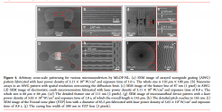
Well super resolution lithography is quite a nascent field so of course the first iterations are going to be rough, even tough those lines looks hideous those are like 16X the wavelength resolution. When Perkin Elmer showed wafers processed with their microaligner for the first time one of the comment was "Those are the most horrible edges I've ever seen", they solved those issues later. More worrying is how scalable it is, because these results may be due to photoresists or some problem in the technique that can be solved. E-Beam lithography produces very nice lines at very good resolution but not scalable, it is not intended for volume production.


1666866749192.png
1666866896634.png
 

tphuang

Lieutenant General
Staff member
Super Moderator
VIP Professional
Registered Member
Isn't that not too far from Fugaku computing power? These guys are building premier supercomputers as if they are public utilities.
Not sure, but 300 PFLOPS is not that much these days. For example, XPeng is building a 600 PFLOPS training center for its autonomous driving training. I think Tesla built a 1.8 EFLOPS training center. But overall, China is definitely building its supercomputing clusters like hot cakes. You hear a lot about smart city and data centers everywhere in China. That's just not something people really care about here in America. So regardless of how much US admin restricts China, it doesn't solve the fundamental issue that there is not a lot of desire in America for large smart data centers outside of large gov't facilities and tech giants. Whereas in China, every municipality is looking for their own large computing center. That might be a little wasteful, but does offer a great resource for local R&D.

For example, Google has 9 EFLOPS of AI super computing power and Meta has 5 EFLOPS. That sounds like a lot, but China is aiming for over 200 EFLOPS nationwide by 2023 and 20% additional capacity every year. All this additional super computing power has dramatic effects on people's daily life and new industries and such.
Good article.

Please, Log in or Register to view URLs content!
Thanks, that's quite a bit of advancement. However, 36% is still quite a long way from 100%. Chinese tools makers really can't expand their production fast enough. Hoping the recent sanctions don't slow down expansion plans. At least I haven't noticed any slow downs.
 

caudaceus

Senior Member
Registered Member
Thanks, that's quite a bit of advancement. However, 36% is still quite a long way from 100%. Chinese tools makers really can't expand their production fast enough. Hoping the recent sanctions don't slow down expansion plans. At least I haven't noticed any slow downs.
Quick question is scaling the main issue or developing the tools is?

In other words is it scaling from 1 to 100 or jumping from 0 to 1?
 
Status
Not open for further replies.
Top