supercat
Colonel
Does the manufacturing of PCB need cutting edge high tech?
Does the manufacturing of PCB need cutting edge high tech?
No. This is not a point of leverage.Does the manufacturing of PCB need cutting edge high tech?
The hits just keep coming. If this doesn't push the Koreans to go 100% at de-Americanizing their production line, then nothing will.More turbulence ahead for semiconductor industry, many semiconductor companies might be forced to be sold or relocated or exited certain market.
Bro,
Facts you cited are not correct:
- N+3 is similar to tsmc N6 (on paper). But in reality, N+3 built with DUV will be inferior in terms of overall yield/quality than N6 built with EUV.
- Intel's 'N' (HVM) node as of Oct 2022 is Intel4. Intel4 output volume is now bigger than SMIC N+1
- Intel4 will reach output volume > the entire SN1 wafer output by late 2024.
- Intel4 has higher transistor density than tsmc N4.
So, your claim that 'N+3 is N5' & that 'SMIC will be ahead of Intel by 2 generations' are incorrect.
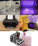
There is not clear cut answer to that question, all depends the complexity of the PCBs you want to make and what volume you want. Very simple LDI single layers ones you can make a few dozens at a home with simple tools:Does the manufacturing of PCB need cutting edge high tech?


I know that Chinese fabs are testing and verifying SMEE scanners, is all a black box, but It could be that the first batch of immersion scanners are going to Huawei to the new fabs that they want to make, in their website they say they are going to make 28nm chips and looks like they don't have a high volume output at the beginning.I thought it would be good to summarize the present state of the Chinese lithography industry at this point of YOOL 2022:
DUV:
EUV:
- The SSA800 has met expectations (or disappointed them, depends who you ask) and delivered to customers for 28nm production. It is roughly comparable to an ASML NXT:1980Di. China has achieved completely indigenous 28nm volume production.
- The SSA800 is expected to be used in 14nm production through multipatterning next year.
- A follow-on DUVL machine (name unknown) using a more powerful light source and improved workbench for single exposure production of 22nm and multipatterning of 7nm (perhaps 5nm?) is expected Soon™. Expected to be comparable to ASML NXT:2050i.
I'd welcome the inputs, thoughts, and critiques of knowledgeable members like @WTAN, @tokenanalyst, and @FairAndUnbiased.
- There were some rumours of a 150W DPP EUVL tool supposed to be released around now. Obviously, no such thing has materialized, which means it's A) very secretive or B) as I suspect, DPP is not a viable path to commercial EUV.
- Everything about LPP EUV is a black box (at least in comparison to DUV). No word on the status of the CO2 laser, the optics, etc. All we "know" is that a machine should be ready around 2025.
- SSMB is a very interesting dark horse, but I don't think it's in the running for China's first generation EUVL. If it lives up to its promise, it would be a vast improvement over LPP EUVL and China would gain enormous advantages from getting to it first.

That's been the case since 2021 (I believe the machines were delivered early 2021 or late 2020). If they still haven't ramped up production, that could indicate problems.I know that Chinese fabs are testing and verifying SMEE scanners, is all a black box, but It could be that the first batch of immersion scanners are going to Huawei to the new fabs that they want to make, in their website they say they are going to make 28nm chips and looks like they don't have a high volume output at the beginning.
Could you post the source for this?Research information says the CAS is working with a least two players to develop the high power lasers for EUV application.
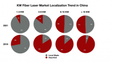
The charts you posted show encouraging progress, however, those are fibre lasers, not the CO2 MOPA laser used in LPP.In term of high power lasers the Chinese laser industry is growing pretty fast.
Could you post the source for this?
According to this paper:
In order to improve the ability to independently develop high-performance chips, my country has started EUVL research. The project "7000 W axial fast flow CO 2 laser" jointly undertaken by Wuhan Optics Valley Keweijing and Huake has successfully passed the acceptance and reached the international advanced level, forming a series of 1 kW–10 kW fast axial flow CO 2 laser products. It will be developed in the direction of high-power and high-purity radially polarized fast axial-flow CO 2 lasers [ ] . Huazhong University of Science and Technology has successfully developed a series of cross-flow CO 2 lasers with powers of 2 kW, 5 kW and 10 kW, and successfully commercialized more than 100 sets of high-power cross-flow CO 2 laser processing systems [ ] . Pan Qikun et al. [ ] proposed a laser power stabilization method and laser power amplification system, which effectively improved the stability of the output narrow pulse width laser power and pulse energy after CO 2 laser amplification. After that, the team proposed a dual-wavelength laser coaxial output system, which solved the problem that tunable CO 2 lasers could not output dual wavelengths at the same time, and improved the use of dual-wavelength CO 2 lasers in EUV lithography light sources in the MOPA system . power extraction efficiency and consistency of dual-wavelength CO laser beam quality, polarization degree, and transmission direction in [ ] . Shanghai Institute of Optics and Mechanics proposed a molten droplet generation device for EUV light sources, and then proposed an integrated tin raw material canning system for droplet targets in EUV light sources, which can obtain more uniform melting tin, and its high degree of integration, safe and convenient operation, suitable for the canning of EUV light source tin raw [ ] . Yin Peiqi et al. [ ] conducted extensive research on the characteristics of plasma generated by laser pulse irradiation of droplets, and carried out experimental research on Nd:YAG laser-induced droplet plasma by using direct imaging method and shadow method, and analyzed the droplet plasma. The expansion characteristics of the body plume and the movement of the droplets under the laser action. Sun Qin et al. [ ] carried out research on the diagnosis method of tin plasma characteristics irradiated by pulsed laser, and used Langmuir probe to obtain the time evolution of electron temperature and electron density of tin plasma generated by irradiation with different laser energies. Qi Lehua et al. [ ] conducted research on the uniform generation and shape change of droplets. Through numerical simulation and experimental research on the uniform droplet spraying process, it was found that the droplet jet velocity mainly depends on the spray pressure, and the droplet flow uniformity mainly depends on the spray pressure. Depending on the disturbance frequency and disturbance amplitude, the pressure field of the jet changes periodically. Xiao Yuan et al. [ ] used a self-developed metal droplet generation system to analyze the influence of impurities attached to the nozzle wall of the droplet generator on the ejection stability and the effect of process parameters on the uniformity of the droplet. The development has certain reference value. Wang Zhanshan et al [ ]A Mo/Si multilayer spherical mirror suitable for 13.5 nm extreme ultraviolet light was developed. The diameter of the spherical mirror is 125 mm and the radius of the curved surface is 143 mm. The uniformity of the multilayer film thickness of the spherical mirror is below 0.8%. The diameter of the circular mirror is 300 mm. The Shanghai Institute of Optics and Mechanics successfully produced a 13.5 nm EUV mirror in 2011, with a test reflectivity of 67.8%, close to the theoretical maximum value of 73.7% [ ] . Wang Xun et al. [ ] used the reactive magnetron sputtering process, combined with the "hysteresis loop" relationship composed of sputtering voltage and oxygen flow rate, to prepare a metal oxide protective layer with excellent purity, roughness, density and uniformity. . Sun Shizhuang et al. [ ] used molecular dynamics model to simulate the probability of reflection and re-sputtering during the deposition of Mo/Si atoms, and prepared multilayer film samples on substrates with different tilt angles through magnetron sputtering experiments to verify the simulation. Simulation results of the model. Sun Shizhuang et al. [ ] obtained the relationship between air pressure and target-substrate distance and film surface roughness. Today, we are in the process of upgrading and transforming DUV to EUV lithography. Through the continuous efforts of domestic researchers, active learning and reference of foreign advanced technologies, coupled with the support of strong comprehensive national strength, my country's lithography technology and semiconductor industry will definitely enter the fast lane of development. And gradually shorten the gap with the international advanced level.
This company is developing CO2 lasers that could be used in Laser Produced Plasma application for EUVL, basically making it the second commercial company in China involved in the EUVL project. Also there are a lot of other achievements in this paper.
There are companies that develop MOPA lasers in China, like Raycus, so working with those to develop a high power system is maybe path. There could be other pathways, just because someone did it in some way that doesn't mean is the only way.The charts you posted show encouraging progress, however, those are fibre lasers, not the CO2 MOPA laser used in LPP.
