Chinese semiconductor industry

Status
Not open for further replies.

tokenanalyst

Brigadier
Registered Member

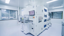
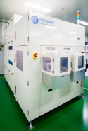
Huaying Micro 12-inch automatic edge corrosion equipment was successfully delivered​


On September 18, 2022, the 12-inch automatic edge corrosion equipment produced by Wuxi Huaying Microelectronics Technology Co., Ltd. was delivered to customers on time.

The equipment can achieve precise etching of the wafer edge, with a precision control of ±0.1mm; at the same time, it saves 50% of the process time, and improves the process safety and the ESH index of the process; in addition, it greatly reduces the chemical corrosion gas. It can save 90% of ultra-pure water and more than 50% of chemical liquid, which can save the cost of ultra-pure chemicals worth millions of yuan each year for customers and enterprises, as well as the treatment cost of their production waste liquid.

Since its establishment, Huaying Micro has always adhered to the company's entrepreneurial philosophy of "technology and environmental protection coexist, innovation and green mountains and green waters coexist". All of the company's R&D designs abide by the tenet of "innovation and environmental protection" first. It is committed to solving many problems such as water resources, environmental protection, and lack of independent innovation technology that the country will face in the development of the semiconductor manufacturing industry. In the future, Huaying Micro will continue to provide the industry and customers with more environmentally friendly, green and advanced semiconductor manufacturing equipment.

Huaying Micro 6/8 inch automatic passivation equipment was successfully delivered​

Release date: 2022/08/17
On August 15, 2022, the 6/8-inch compatible fully automatic passivation equipment produced by Wuxi Huaying Microelectronics Technology Co., Ltd. was successfully delivered to customers.

This is Huaying Micro's first fully automatic multi-cavity passivation equipment. The equipment has the characteristics of good process repeatability and high film-forming efficiency, and greatly reduces the process cost, and solves many long-standing problems in the existing passivation process and equipment.

The new passivation equipment shipped by Huaying Micro is equipped with multiple chambers, which greatly improves the production efficiency. At the same time, it can realize dry in and dry out, online recovery and recycling of used chemical solvents, etc., which can save more than 50%. Process time, save more than 90% of chemicals, save a lot of production costs for enterprises, and better protect resources and protect the environment.

Huaying Micro is committed to the design and manufacture of industry-leading, green and environmentally friendly new semiconductor manufacturing and production special cleaning equipment and new processes. The coexistence of technology and environmental protection, innovation and green mountains and clear waters are the foundation of Huaying Micro's foothold in the field of semiconductor manufacturing. Huaying Micro uses its own original technology, and strives to bring the best experience to customers.
(Contributed by Xu Lu)
1666737867566.png1666738021565.png

Please, Log in or Register to view URLs content!
 

mmbro

New Member
Registered Member
What the article does not delve into, is the rationale or possible outcomes of China not having the best chips, will that be enough for the US to maintain a lead over China in AI for example?
MSM likes to portray that AI etc need super-duper 5nm or even 3nm, but in reality most AI used in a system such as transportation centers, hospitals, computing etc require just 14nm quite fine as most of the application are integrated into an equipment that is on-site, stationary (or even transportable with a reasonably big size).. it's not a smartphone
 

tokenanalyst

Brigadier
Registered Member
| Focuslight Technology Launches High Power Semiconductor Laser Side Pump Module SP17 and SP18


Xi'an, China – October 11, 2022 – Focuslight Technology, a global supplier of high-power semiconductor lasers and micro-optics, has released
Please, Log in or Register to view URLs content!
. These two products can achieve peak power output of 30kW and 5kW respectively, while achieving higher Small Signal Gain (SSG) (SSG: SP17>55, SP18>30) and better fluorescence distribution uniformity ( >90%), the core indicators have reached the world leading level. It can be used for high-power solid-state laser pumping, and ultimately used in advanced manufacturing fields such as material precision processing, surface treatment, and pan-semiconductor manufacturing.

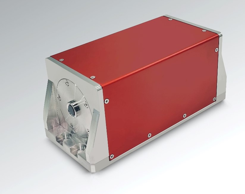
editor1665451567128006.jpg

Focuslight Technology High Power Semiconductor Laser Side Pump Module SP17

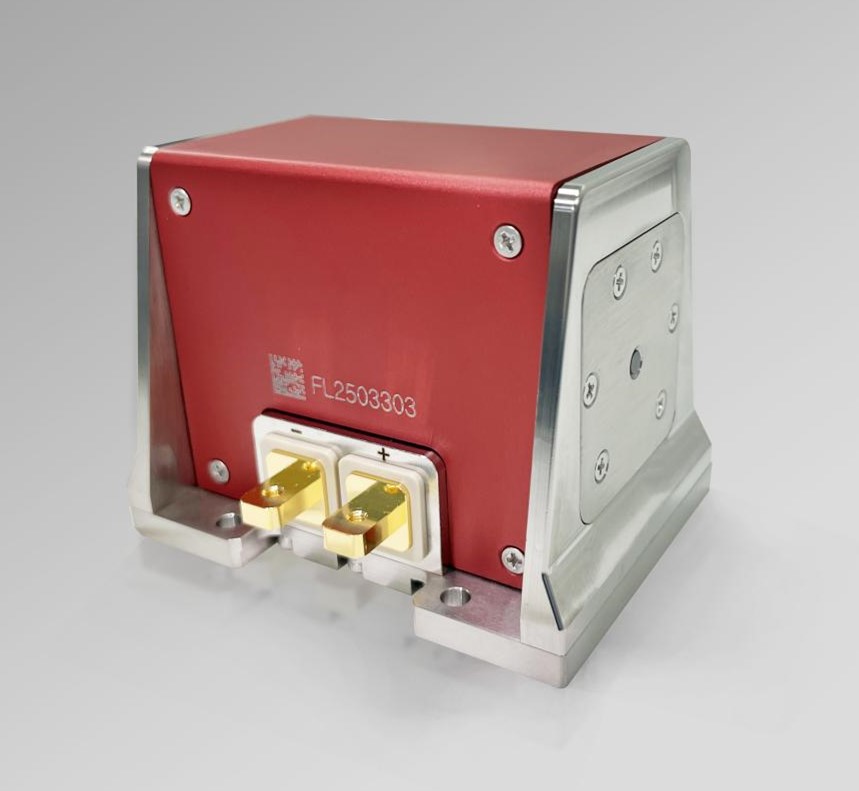
editor1665451585437639.jpg

Focuslight Technology High Power Semiconductor Laser Side Pump Module SP18

Semiconductor laser-pumped solid-state lasers (DPSSLs) have the advantages of high power, high beam quality output, less thermal effect, high efficiency, and compact device structure. They have gradually replaced traditional lamp-pumped lasers and gas lasers, and are widely used in many advanced manufacturing. field. As the core pump source of the solid-state laser, the semiconductor laser side pump module directly determines the performance and reliability of the solid-state laser.
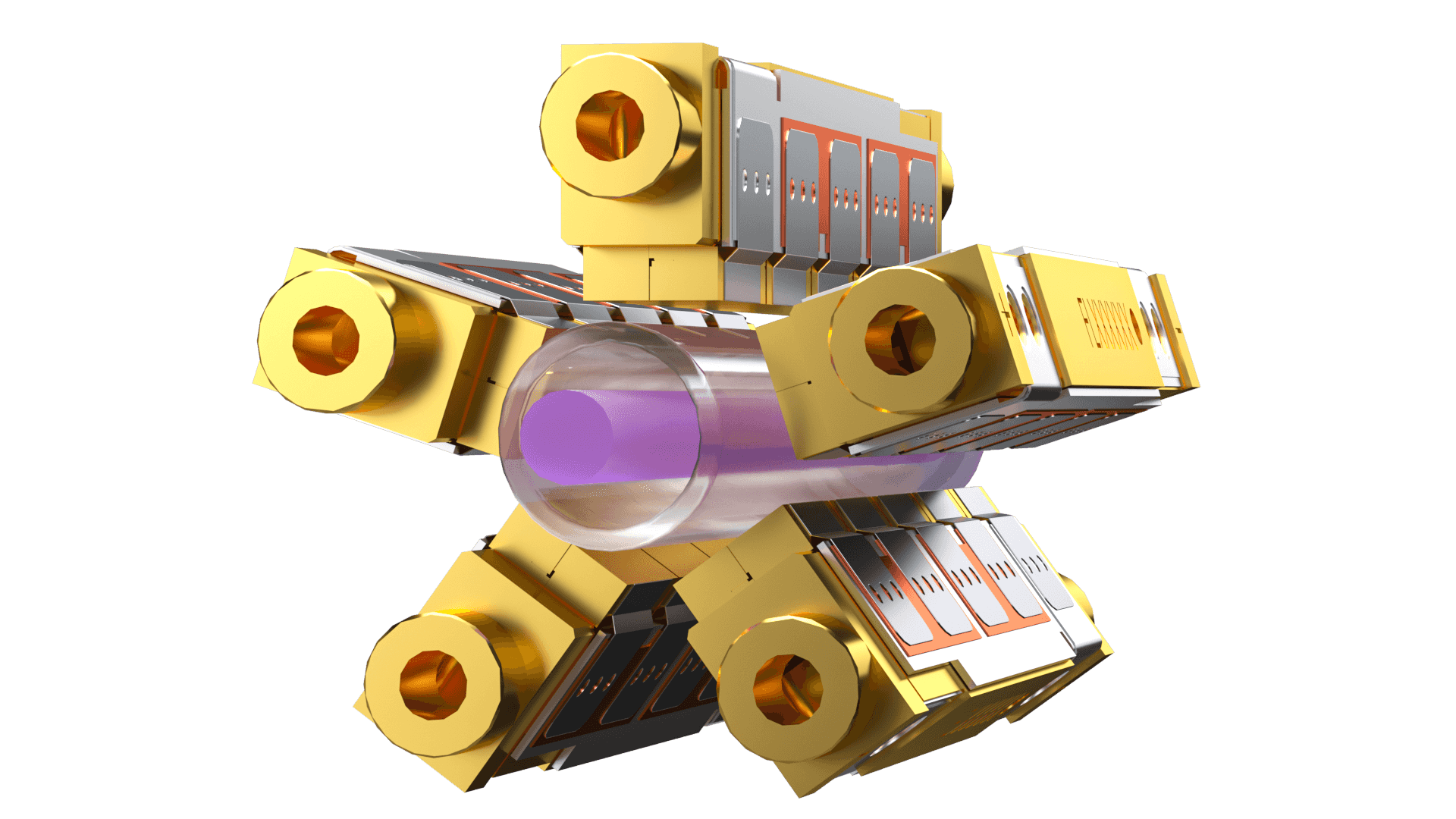
The SP17 and SP18 high-power semiconductor laser side pump modules released this time use the leading high-power semiconductor laser of Focuslight as the core component, use a five-phase pump structure, and use unique optical design and waterway design, as well as effective means to control ASE (Amplified Spontaneous Emission) effect to achieve high pump peak power, high gain and high uniformity of fluorescence distribution. As the gain increases, if no corresponding measures are taken, the high-peak power pumping module will produce a serious ASE effect, resulting in gain saturation and high SSG cannot be obtained. The SP17 and SP18 side pump modules take effective measures to suppress the ASE effect, so that the SSG of the SP18 can reach more than 30, and the SSG of the SP17 is more than 55.

editor1665451617279898.png

Five-phase pump structure diagram

Please, Log in or Register to view URLs content!
 

paiemon

Junior Member
Registered Member
Industry sources said that China's top foundry SMIC and other domestic peers are expected to stay put at the 28nm chip era as their R&D momentum is being greatly deterred by the US restrictions on China-bound exports of advanced manufacturing equipment and related software tools and services.
I thought based on previous posts it was fully domestic at this point could support up to 28 NM while de-Americanized could support up to 7 NM based on chips SMIC has taped out and the interview with the LAM employee who stated that SMIC has de-Americanized capabilities at that node. If the R&D momentum is affected it would for future nodes that have not yet been designed and validated, and if we want to push the definition of R&D we can say that expansion at those nodes they have already researched up to N+3 may be bottlenecked since non-US suppliers will have even more backlogs if TSMC and friends decide to de-Americanize where they can. Maybe Digitimes is expecting that China will only source domestically to arrive at the 28NM bottleneck statement? I thought Digitimes was supposed to be an industry focused publication, weird to see them come up with such a poorly researched statement.
 

tphuang

Lieutenant General
Staff member
Super Moderator
VIP Professional
Registered Member
I thought based on previous posts it was fully domestic at this point could support up to 28 NM while de-Americanized could support up to 7 NM based on chips SMIC has taped out and the interview with the LAM employee who stated that SMIC has de-Americanized capabilities at that node. If the R&D momentum is affected it would for future nodes that have not yet been designed and validated, and if we want to push the definition of R&D we can say that expansion at those nodes they have already researched up to N+3 may be bottlenecked since non-US suppliers will have even more backlogs if TSMC and friends decide to de-Americanize where they can. Maybe Digitimes is expecting that China will only source domestically to arrive at the 28NM bottleneck statement? I thought Digitimes was supposed to be an industry focused publication, weird to see them come up with such a poorly researched statement.
I think the SMIC SN1 fab is pretty opaque and same with ICRD production line. My guess is that China at this point is fully domestic up to 28 nm, but can produce things at low yield at 14 nm. So, I think the fully domestic line at ICRD is probably at 14 nm or maybe even N+1. I think SMIC is keeping that SN1 fab intentionally opaque to not attract more attention. Just imagine the hysteria and pressure on Dutch gov't if SMIC is found to be able to produce 5nm chips with the most recent ASML machines. After all, SMIC is still needing ASML scanners to fully expand its SN1/SN2 operation.

Overall, it's probably not easy for Digitimes to confirm exactly where SN1 is at since SMIC tries to keep it secretive and the fab itself is not producing very high volume. So, they are just going with "industry sources" that are outside of China.

The other possibility is that since China is expanding the 28nm+ sector of the market, they just assume China is abandoning the more advanced segment of the market.
 

Maikeru

Major
Registered Member
On the back of reading this thread and not understanding too much of it, I have started reading this:

Please, Log in or Register to view URLs content!

So far a fascinating canter through the early history of chip-making and the global chip industry, including its strategic context, and I now understand a lot of terms used in this thread that I didn't before.
 

weig2000

Captain
On the back of reading this thread and not understanding too much of it, I have started reading this:

Please, Log in or Register to view URLs content!

So far a fascinating canter through the early history of chip-making and the global chip industry, including its strategic context, and I now understand a lot of terms used in this thread that I didn't before.

The guy has spent five years to do research and interviews for the book. The book is published at the right time (now). He is busy giving interviews these days.
 

TK3600

Major
Registered Member
Not that if you do not own the tools the work that you made with the tools belongs to the US government.

Taiwanese and Korean IC chip manufacturing companies that purchase lithography scanners and equipment for etching, ion implantation, deposition, metrology etc from US companies to from other foreign companies that make such equipment with US content do own those tools that they purchased. It is just that if they do not abide by US geopolitical terms, the United States will decide not to supply them with those tools anymore. And they might decide not to purchase the chips made by American made and American-content possessing tools, which will also hurt them because the US and US companies over which the US government has full jurisdiction are a significant portion of their market.

And I fully agree with you with regards to it being much more important to actually be able to make the semiconductor and IC chip manufacturing equipment than it is to just be able to use foreign supplied equipment and be able to make IC chips with them much better than the tool makers themselves could do. That is why I deem it extremely arrogant when people here scoff at Japan not commercially producing less than 40 nm node logic chips, when Japan integrates the production of semiconductor and IC chip manufacturing equipment, largely or entirely free of foreign content, and also makes chips using their own equipment better than any other country.

It is Japan that has the best integration of the domestic supply chain for semiconductor substrates, IC chips materials, making-equipment, and IC chips themselves than any other country. Saying that fact does not make on a lover of the Imperial Japanese Army or a weaboo. It is just a matter of fact. China itself actually decently integrates that supply chain, certainly much better than Taiwan and Korea does, and China could definitely make IC chips as well as they could if China had access to EUV equipment. But due to US domineering interests at keeping China down, they have ensured that ASML does not supply EUV machines, and they are trying to ensure that as much as possible that NO American company and those of American allies supply any chip manufacturing equipment and materials to China that China doesn't itself produce that is comparable quality or better than what the US and its allies produce.

As I and others have said as nauseum and will keep reminding people periodically in this forum, faced with these realities, being that China's geopolitical interests and stature are so much larger than South Korea (no disrespect to South Korea and Koreans), China must ensure that the entirety of supply chains to produce semiconductors and IC chips and their equipment and special materials be located within China, and the same applies for any item of technology that is worth producing - China must at least demonstrate the capability of producing them. From this forum, I have been well informed that the greatest weakness with regards to China is lithography scanners and steppers. If China can replicate or come close to replicating the most advanced DUV machines that ASML produces qualitatively, it is GAME OVER FOR THE UNITED STATES as far as the semiconductor and IC chip containment policy of China.
Can Japan create a whole 14nm fab from lithography to cleaning, fabrication, software design and everything else? As of now I think Chinese full domestic 14nm is the best a single country can do.

If China pull a USA on Japan can they do a fab from ground up? No rare earth and etc. What about rest of the world combined? I think we all know the answer. ONLY China can pull off a complete supply chain from minerals to machine to fab.
 
Last edited:
Status
Not open for further replies.
Top