
This from CETC alone and my guess is that they have their own MOCVD equipment for this kind semiconductors as they always do.The US recently sanctioned Gallium Oxide to prevent China graduating to next generation technologies in EV, power and battery sectors. These 2-4 inch Ga2O3 wafer ingots are leading edge R&D and large enough for commercialization. Until this news, I was under the impression that China's MOCVD systems were generations behind and was the main reason the US imposed multi-lateral sanctions of Ga2O3. Can somebody clarify the exact state of China's 4th gen semiconductor research, because this sounds like China is less than 2 years behind the world leader Japan?
CAS is also development semiconductor equipment for this kind of gallium oxide and probably the plan to start commercialization as soon enough.
We also can't forget the one of the stronger areas of AMEC is MOCVD, so it maybe not that difficult to them to make equipment for this type of material if there is market for it.Research and development of Manufacturing equipment for Gallium Oxide Substrates.
Interesting story. looks its was not economically possible to mass produce this material without some change in the equipment used.
View attachment 96034
Wang Gang led the team to solve the key core problems in the industrialization of gallium oxide semiconductor materials.
View attachment 96035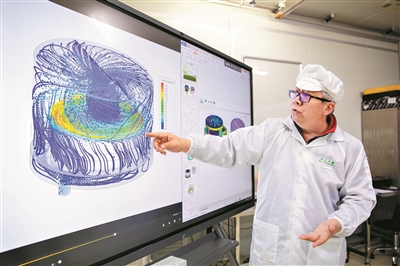
Wang Gang's team used digital modeling, digital twin and other technologies to visualize the reaction chamber.
View attachment 96037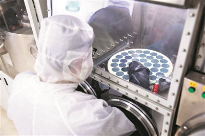
The research results on the national list are behind the tenacity of Wang Gang's team for more than ten years.
Recently, the 2022 "Technology Innovation China" annual conference with the theme of "Technology Self-reliance, Self-reliance and Entrepreneurship Drives Development" was held. At the meeting, the China Association for Science and Technology released the 2021 "Science and Technology China" series of lists. Among them, the "Leading Technology List" has selected 100 leading technologies with broad application scenarios and high economic and social benefits in six major fields, including biomedicine, resources and environment, electronic information, equipment manufacturing, advanced materials, and modern agriculture and forestry.
The "Heteroepitaxial Growth Technology and Core Equipment of Large-sized GaO Single Crystal Thin Films" independently developed by the research and development team led by Professor Wang Gang from the School of Electronics and Information Engineering (School of Microelectronics) of Sun Yat-sen University for more than ten years is the only project selected by universities in Guangdong Province. , is also the only selected project in Guangzhou. The technology developed by Wang Gang's team will form an industrial breakthrough in the field of emerging ultra-wide bandgap power semiconductor materials in China and even in the world, and will greatly promote the development and industrialization of gallium oxide-based power electronic devices in China.
The research results on the national list are behind the tenacity of Wang Gang's team for more than ten years. "Every time a door is opened, it takes constant exploration and repeated trial and error to find the next door." Wang Gang sighed to reporters.
When the reporter walked into the wide bandgap semiconductor material and device laboratory, generations of large-scale CVD equipment came into view. Wang Gang said that these are all CVD equipment purchased from abroad. "In 2006, we bought back this long-nitride machine from the UK. We had a hard time negotiating for a discount, but it also cost us nearly 10 million yuan." Wang Gang said.
In order to achieve a breakthrough from 0 to 1 in gallium oxide epitaxial materials and core equipment, Wang Gang led the team to develop MOCVD (metal organic chemical vapor deposition) equipment for heteroepitaxial growth of large-scale, high-quality gallium oxide semiconductor thin film materials. Large-scale heteroepitaxial growth process technology of gallium single crystal thin film materials.
"When we went to an academic exchange meeting, we heard Japanese experts share the prototype of gallium oxide power electronic devices. I thought we were equally capable of doing this, and we could go out of different technical paths, so we immediately started research after returning to China, and Heteroepitaxy was attempted with sapphire as the substrate." Wang Gang said that in the first two years, they were unable to grow thin film materials on the sapphire substrate. This feeling of suffocation and unpleasantness has always been unforgettable for Wang Gang. He also had doubts: Can this research direction really lead to success?
In anxiety and confusion, Wang Gang's team never gave up. Relying on the long-term research experience in nitride semiconductor components, they retrofitted an old MOCVD equipment for the production of second-generation semiconductor materials, and uniquely designed the reaction chamber of the semiconductor equipment. Over the past ten years, the team has continuously adjusted the process, parameters and design plans, and has accumulated experience in nearly 10,000 failures. In the end, they realized the independent development of MOCVD equipment for epitaxial growth of gallium oxide single crystal thin film materials, and they used the self-developed MOCVD equipment to grow crystals with high quality and uniform crystal orientation on large-scale heterogeneous substrates such as sapphire, silicon carbide and silicon. Good 4-8 inch ε phase gallium oxide single crystal film.
Multidisciplinary integration makes "black box" visualization
Wang Gang is filled with idealistic feelings. He told reporters that his goal in life is to develop better domestically produced equipment, and then grow better semiconductor materials.
")
