You are using an out of date browser. It may not display this or other websites correctly.
You should upgrade or use an alternative browser.
You should upgrade or use an alternative browser.
Chinese semiconductor industry
- Thread starter Hendrik_2000
- Start date
- Status
- Not open for further replies.
not really related to the semiconductor world (naura talking to us gov reminded me of this), but have there been news about us audits on chinese companies? in hk iirc
The US is clearly trying to pull the same stunt as they did with Samsung, TSMC pulling their customer lists and detailed delivery numbers. If Naura management is retarded enough to release such info, to maintain their business advantages, then prison sentences have to be given. China needs to step in immediately and make it crystal clear to all of China's companies, in all fields that there can be zero cooperation with the US government without China's prior approval and direct involvement. Honestly, I find this news hard to believe because it seems so incompetent of China's government. There must be something behind this news we don't know of.The more Naura talks with US government representatives the worse it will be. They should just extricate themselves from any dealings with them. They will want to know all their suppliers and customers, so they can more easily contain and kill them if necessary.
JiCui Huake semi-automatic wafer measuring machine was officially delivered to the leading international packaging company
On August 2nd, the ZEUS-W300 semi-automatic wafer measuring machine of JiCui Huake completed the packing and delivery, and was officially delivered to the leading international packaging company.ZEUS series wafer measuring machines are independently developed by JCHUAKE Measuring Equipment Division. They are aimed at high-precision optical three-dimensional topography measurement in the IC industry. ZEUS-W300 semi-automatic and ZEUS-W300A automatic products have been formed, serving compound semiconductor, silicon-based The front/rear section of the device, LED, optical communication and other fields.
The main features of ZEUS series wafer measuring machine are as follows:
(1) Modular definition + personalized customization
Through a variety of combinations of 3D&2D probes, sensors, robotic arms, etc., the optimal non-contact measurement solution is provided to solve customers' troubles in complex measurement; the built-in motion execution system can be used according to customers' requirements for different motion configurations and different motion strokes. Needs, easy combination to achieve personalized customization.
(2) Self-developed measurement software driven
ZEUS series wafer measurement machine adopts the measurement software independently developed by JCI, which has a number of unique advantages.
- Adapt to a variety of probes and controllers;
- Supports measurement of various wafers such as light wafers, patterned wafers, wafers on saw frames, and multi-layer wafers, providing measurement functions such as wafer thickness, roughness, total thickness variation (TTV), total stack thickness, and warpage. ;
- It supports custom measurement process, can automatically take point measurement and save measurement mode and data, and can present various result forms such as data list, 2D drawing, 3D pseudo-color map and so on.
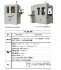
Self-developed measurement software
(3) Powerful white light interference technology The
application of white light interference technology can obtain relevant data of key dimensions such as the 3D topography, surface roughness, TSV and other key dimensions of the wafer surface, which can be used to determine the surface roughness, waviness, Surface topography features such as surface profile, surface defects, wear, corrosion, pore gaps, step heights, and machining conditions are measured and analyzed. The images below show examples of applications of this technology to measure different parameters on several different materials.

Application Cases: Semiconductors, Polished Wafers, Thinned Wafers, Wafer ICs
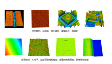
Application cases: 3C electronics, sapphire glass roughness, metal shell mold defects, glass screen height difference
Relax, they probably talked with the Chinese officials first before even considering going to talk with BIS officials.The US is clearly trying to pull the same stunt as they did with Samsung, TSMC pulling their customer lists and detailed delivery numbers. If Naura management is retarded enough to release such info, to maintain their business advantages, then prison sentences have to be given. China needs to step in immediately and make it crystal clear to all of China's companies, in all fields that there can be zero cooperation with the US government without China's prior approval and direct involvement.
Naura also owned Akron (a wafer cleaning company it seems) so maybe related to that.Relax, they probably talked with the Chinese officials first before even considering going to talk with BIS officials.
Haobao's technical team has developed a vertical curing furnace specially used for IGBT module packaging, which can be fully automated, avoid device oxidation, has good temperature uniformity and high cleanliness, and brings great benefits to IGBT power semiconductor packaging manufacturers. High-efficiency, high-yield solutions.

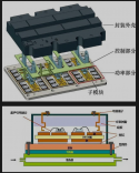
According to reports, the core technical advantages and characteristics of Haobao's IGBT module packaging vertical curing furnace are as follows:
1. Fully automatic production and management, greatly reducing labor.
The equipment adopts a modular structure, which realizes fully automatic and online production such as loading and unloading, baking, cooling, and buffering. The production efficiency is high, and the production capacity can be increased, decreased, and adjusted according to customer needs.
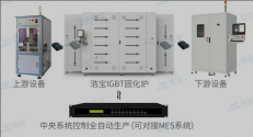
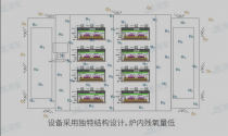
2. Low residual oxygen content to avoid device oxidation
The equipment adopts a unique structural design and has applied for an invention patent, which can ensure that the residual oxygen content is controlled within 1000PPM during the process of transmission, heating, cooling and buffering, effectively avoiding the oxidation of heat-sensitive devices such as metals.
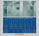
3. High cleanliness to meet the requirements of dust-free production
The equipment has good airtightness, and adopts a high-efficiency filtration and cleaning system, so that the packaging process can reach a thousand-level cleanliness and meet the requirements of dust-free production.
4. High temperature uniformity, good product consistency
The equipment adopts excellent heating and temperature control modules and unique air duct and cavity design, which can ensure high heating efficiency and uniform and stable temperature, so that baking and curing are uniform and product consistency is high.
The fully automatic vertical curing furnace for IGBT modules successfully developed by Haobao has broken through a number of key technical difficulties, and the price is only one-third of the imported equipment, providing power semiconductor manufacturers with more cost-effective packaging and curing equipment and solutions.


According to reports, the core technical advantages and characteristics of Haobao's IGBT module packaging vertical curing furnace are as follows:
1. Fully automatic production and management, greatly reducing labor.
The equipment adopts a modular structure, which realizes fully automatic and online production such as loading and unloading, baking, cooling, and buffering. The production efficiency is high, and the production capacity can be increased, decreased, and adjusted according to customer needs.

2. Low residual oxygen content to avoid device oxidation
The equipment adopts a unique structural design and has applied for an invention patent, which can ensure that the residual oxygen content is controlled within 1000PPM during the process of transmission, heating, cooling and buffering, effectively avoiding the oxidation of heat-sensitive devices such as metals.

3. High cleanliness to meet the requirements of dust-free production
The equipment has good airtightness, and adopts a high-efficiency filtration and cleaning system, so that the packaging process can reach a thousand-level cleanliness and meet the requirements of dust-free production.

4. High temperature uniformity, good product consistency
The equipment adopts excellent heating and temperature control modules and unique air duct and cavity design, which can ensure high heating efficiency and uniform and stable temperature, so that baking and curing are uniform and product consistency is high.
The fully automatic vertical curing furnace for IGBT modules successfully developed by Haobao has broken through a number of key technical difficulties, and the price is only one-third of the imported equipment, providing power semiconductor manufacturers with more cost-effective packaging and curing equipment and solutions.
Probably more related to the magnetic material company that they own. Probably they were buying parts or materials or something from the US and that caught the attention of the national security lunatics.Naura also owned Akron (a wafer cleaning company it seems) so maybe related to that.
The US recently sanctioned Gallium Oxide to prevent China graduating to next generation technologies in EV, power and battery sectors. These 2-4 inch Ga2O3 wafer ingots are leading edge R&D and large enough for commercialization. Until this news, I was under the impression that China's MOCVD systems were generations behind and was the main reason the US imposed multi-lateral sanctions of Ga2O3. Can somebody clarify the exact state of China's 4th gen semiconductor research, because this sounds like China is less than 2 years behind the world leader Japan?2-inch gallium oxide homoepitaxial wafer was successfully prepared by the 46th Institute of Electronics Technology of China
Walking into the busy key laboratory of new semiconductor materials, one after another of single crystal and epitaxial growth equipment comes into view. In these seemingly mysterious devices, white gallium oxide powder gathers and grows silently into a tower, and polished sheets made of it are polished. , epitaxial wafers, and various devices made of them have broad application prospects in consumer electronics, new energy vehicles, UHV power transmission, rail transit and other fields.
As a fourth-generation semiconductor material, gallium oxide can be described as "excellent talent", and the large forbidden band width makes it possible to manufacture semiconductor devices with higher withstand voltage and stronger processing capability with less material. Faced with the important task of independent innovation of gallium oxide, 46 institutes took the lead, broke through the growth technology of 2-inch and 4-inch gallium oxide single crystals, and developed high-voltage epitaxial wafers, laying a solid foundation for mass production of gallium oxide.
For once SCMP had its editorial right and YES China is the only country that can realized a full spectrum indigenization thanks to America of course. 
Editorial by SCMP Editorial
Published: 12:50am, 24 Oct, 2022

Semiconductor chips on a circuit board. Photo: Reuters
Short term, the latest measures by the United States to restrict Chinese access to US semiconductor technology will hurt China at the core of its tech development. Longer term, however, they are short-sighted and are likely to cause problems for the US.
Meanwhile, they do nothing to relieve serious bilateral tension. A ban on US passport-holders or entities working with Chinese chip producers without specific approval can only exacerbate it.
The US Department of Commerce has imposed systematic export licensing controls on dozens of Chinese companies and research institutions. Companies worldwide are barred from selling super computing and artificial intelligence chips to China that were made with US software, machinery or technology.
They reveal the depth of a sense of insecurity that American technology hegemony may be challenged by China, already reflected in the US$52.7 billion Chips and Science Act passed recently by Congress to subsidise R&D and manufacturing.
However, in the longer term it will be difficult for one player to exercise dominance over everything, with different countries enjoying an advantage in developing certain components of the technology chain.
If this resulted in fragmentation of the global technology sector, US companies would suffer, since they benefit most from it. So while the latest measures will cause problems for China, ultimately the negative impact may outweigh any gain for the US in consolidating a dominant position.
The passport ban further undermines the perceived values of the US as an emigrant society that attracts the best and brightest. But China needs to be wary it does not boost a rise of nationalism which, if it were to become dominant, could only self-harm. Indeed, Beijing should adopt an open approach and not take any action to deny people the opportunity to come to China.
Editorial by SCMP Editorial
Tech war a sign of US weakness not strength
- China should not overreact to Washington’s ill-thought-out moves to restrict access to products and talent and instead embrace an open and inclusive approach to boost the development of technology
Published: 12:50am, 24 Oct, 2022

Semiconductor chips on a circuit board. Photo: Reuters
Short term, the latest measures by the United States to restrict Chinese access to US semiconductor technology will hurt China at the core of its tech development. Longer term, however, they are short-sighted and are likely to cause problems for the US.
Meanwhile, they do nothing to relieve serious bilateral tension. A ban on US passport-holders or entities working with Chinese chip producers without specific approval can only exacerbate it.
The US Department of Commerce has imposed systematic export licensing controls on dozens of Chinese companies and research institutions. Companies worldwide are barred from selling super computing and artificial intelligence chips to China that were made with US software, machinery or technology.
The measures also limit exports to China of chip manufacturing tools and technology that Chinese companies could put to their own use.
They reveal the depth of a sense of insecurity that American technology hegemony may be challenged by China, already reflected in the US$52.7 billion Chips and Science Act passed recently by Congress to subsidise R&D and manufacturing.
However, in the longer term it will be difficult for one player to exercise dominance over everything, with different countries enjoying an advantage in developing certain components of the technology chain.
Sharing them can accelerate the technological revolution. Beijing will find it difficult to re-create that alone. But, over time, cutting the second-largest economy out of the chain and isolating China technologically will be a tall order.
If this resulted in fragmentation of the global technology sector, US companies would suffer, since they benefit most from it. So while the latest measures will cause problems for China, ultimately the negative impact may outweigh any gain for the US in consolidating a dominant position.
The passport ban further undermines the perceived values of the US as an emigrant society that attracts the best and brightest. But China needs to be wary it does not boost a rise of nationalism which, if it were to become dominant, could only self-harm. Indeed, Beijing should adopt an open approach and not take any action to deny people the opportunity to come to China.
- Status
- Not open for further replies.
