Chinese semiconductor industry

Status
Not open for further replies.

ansy1968

Brigadier
Registered Member
Please, Log in or Register to view URLs content!

It has been posted on a major Chinese publication and has been trending on Baidu for a while.

This is a tremendous achievement for a fellow forum member. I can’t emphasize it enough.
Sir to tell you the truth I'm one of his early fan...lol and when he decided to join this forum, I was ecstatic, he has enhance the credibility of this forum. :) especially his famous quote "Physics is the same in Amsterdam as well in Beijing"
 

tokenanalyst

Brigadier
Registered Member

"Fuxiang Optics" released ZURO series spectrometers to help localization of China's semiconductor industry​


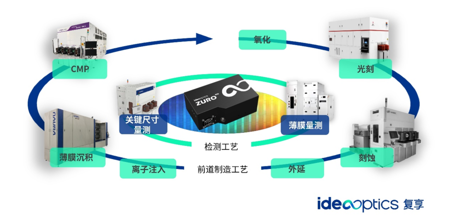
In September 2022, Shanghai Fuxiang Optics Co., Ltd. (hereinafter referred to as "Fuxiang Optics") completed in-depth grinding and production line verification with head customers. It took one year to complete the ZURO series of spectrometers for etching application scenarios. Product development and mass production introduction provide the integrated circuit industry with spectral detection solutions for 6-, 8-, and 12-inch etching processes.

907470888429.6113857237827099.5021.png


ZURO series spectrometers match the semiconductor industry standards and meet the needs of multiple application scenarios such as metal etching, single polysilicon etching, compound etching and high-speed cleaning. This series of products has the advantages of high sensitivity and high signal-to-noise ratio. The maximum dynamic range of single frame acquisition exceeds 40000:1, which is better than similar foreign products, and can effectively extract weak signals in deep holes and polysilicon etching process. In addition, the software equipped for ZURO series spectrometers, ideaEPD is a Fab process-specific software developed by Fuxiang Optics in-depth customer application. It supports custom endpoint algorithms, process endpoint analysis, high-speed sampling monitoring, etching depth monitoring and other functions. Realize simultaneous monitoring of up to 10 chambers. Fuxiang Optics has completed the domestic verification and mass production preparation of ZURO series products, and can carry out differentiated customized development for customers to solve the security problem of key optical components supply for leading customers. At present, Fuxiang Optical's multi-series spectral module products have been verified, produced and ordered by a number of semiconductor head customers. With the continuous deepening of demand response and the continuous optimization of engineering parameters, Fuxiang Optics has gradually entered the stage of high volume from the initial stage, and used spectral hard technology to help the development of the industry.

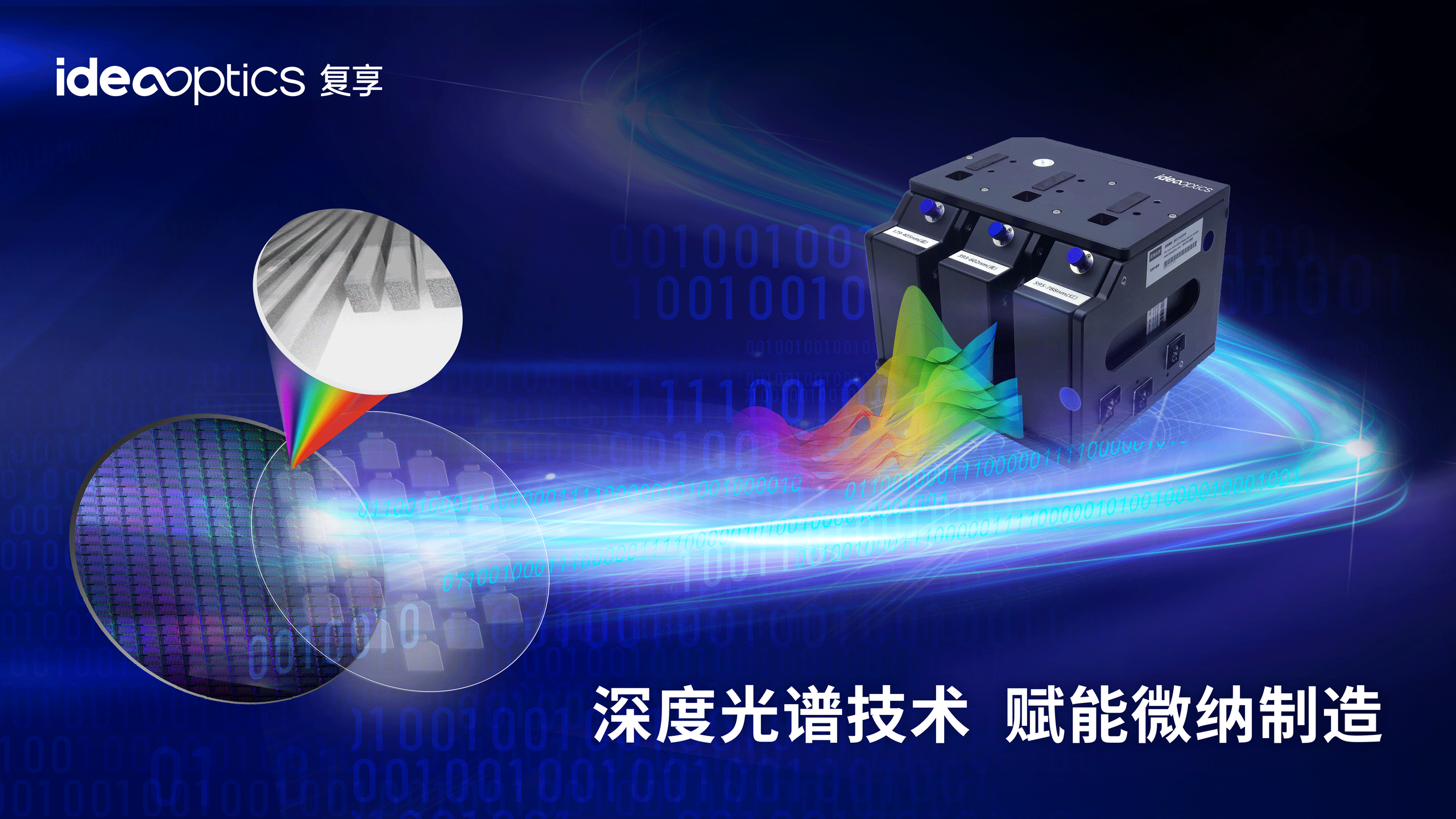
Fuxiangguang has been studying for ten years and has been deeply involved in the field of micro-nano optoelectronics, developing intelligent full-spectrum technology, focusing on the integration of photonics and artificial intelligence, forming an algorithm-driven deep spectrum platform, and becoming China's leading wafer-level manufacturing and quantitative Spectrum module supplier for key components of testing equipment.

The founding team of Fuxiang Optics was born in a senior photonics research laboratory in China. During its development, it has further absorbed well-known researchers and semiconductor industry experts in the field of micro-nano optoelectronics at home and abroad, and has owned nearly 100 intellectual property rights.

It is worth mentioning that Fuxiang Optics was approved to establish the "Shanghai Micro-nano Process Intelligent Inspection Engineering Technology Research Center" in 2019, which is the first application platform in China to carry out research on micro-nano process optical quantity detection technology in the semiconductor field. In order to further explore the basic technology of optical detection in the field of integrated circuits, the company will jointly establish the "Photodetection and Optical Integration School-Enterprise Joint Research Center" with Fudan University in 2021, and is committed to tackling more cutting-edge common key technologies and processes in the micro-nano manufacturing industry. question.
434001284228.7881427252957973.1892.png


According to Fuxiang Optics, with the continuous improvement of advanced integrated circuit manufacturing processes and the rise of new optoelectronic chip applications, the demand for quantitative inspection of wafer manufacturing processes has become increasingly prominent. The existence of the optical diffraction limit makes it difficult for imaging technology to meet the needs of industrial development. Spectral analysis technology has already existed in various micro-nano manufacturing and quantity detection equipment, and has become one of the key technologies supporting the manufacturing process of integrated circuits and optoelectronic chip industries.

Semiconductor equipment is the foundation of the semiconductor industry. Front-of-wafer manufacturing is the most important stage in the semiconductor process. In-process and inter-process control of photolithography, thin film deposition, etching, doping, surface treatment, etc. requires the use of a variety of optical and electrical inspection methods, which are the key to ensuring wafer production yield. With the improvement of process accuracy, the proportion of optical inspection will be further expanded. Looking at the quantity detection equipment in the current integrated circuit manufacturing process, it is inseparable from the depth spectroscopy technology. According to the industry research report, at present, the localization rate of semiconductor equipment in my country is less than 10%, key components are less than 1%, and spectral modules are almost zero. "Comprehensive localization of the industrial chain" has become a major theme of this era.

As a leading company in the domestic optical field, Fuxiang Optics provides various spectral modules and quantitative detection solutions in chip manufacturing process control. Through ten years of industry accumulation, the company has more than 3,000 high-quality customers, successfully entered the supplier list of leading companies in the semiconductor industry, and formed exchanges and cooperation with more than 170 semiconductor, high-end materials, and biopharmaceutical companies.

Enabling micro-nano manufacturing in China will be the top priority of Fuxiang Optics for a period of time in the future. Dr. Yin Haiwei, founder of Fuxiang Optics, said that in the next year, the company will continue to focus on the quality improvement, technical iteration and capacity expansion of high-end spectral modules to further meet the needs of downstream equipment companies.

Please, Log in or Register to view URLs content!
 

tokenanalyst

Brigadier
Registered Member

6.5 billion silicon carbide project landed in Nanjing!​


On September 1, Nanjing Jiangbei New District held a signing meeting for key industrial projects in the golden autumn with the theme of "Investing in Jiangbei for a Win-Win Future". 32 industrial projects were signed at the meeting, with a total investment of 45.5 billion yuan. Among them are a number of key projects such as Superchip Semiconductor, Kaitu Pharmaceutical, SDIC Investment Promotion, and YOFC Guangfang.

It is understood that the key technology research and development and industrialization project of the third-generation semiconductor silicon carbide substrate with a total investment of 6.5 billion yuan was also signed at the meeting. The main body of the project is Jiangsu Chaoxinxing Semiconductor Co., Ltd. ”).

According to the data, Chaoxinxing was established in 2019 by Dr. returnee. It is a leading third-generation semiconductor company in China. It is committed to the research and development and industrialization of 6-8-inch silicon carbide substrates. It has more than 20 years of silicon carbide technology accumulation and Industrialization experience. Through the introduction of technical talents and experts, the company integrates advanced technologies from the United States, Europe, Japan and other countries, continuously iteratively upgrades and surpasses itself, and completes the integration of many core fields such as equipment, crystal growth, processing, and testing, and realizes my country's 6-inch silicon carbide substrate. A new breakthrough in the international arena.

According to the official Weibo report of "Nanjing Jiangbei New District" in March this year, Yuan Zhenqian, co-founder of Superchip, revealed that their third-phase expansion plan has been launched, with a planned production capacity of 300,000-500,000 pieces, which is 15-25 times the current production capacity. In November 2021, Superchip has completed hundreds of millions of yuan in Series A financing. This round of financing was led by CMB International, followed by Huaye Tiancheng and Softbank China, and Tongchuang Weiye continued to make additional investment as an old shareholder. At present, Chaoxinxing’s B round of financing has also been launched, and it is expected that there will be two rounds of financing this year.
 

FairAndUnbiased

Brigadier
Registered Member

"Fuxiang Optics" released ZURO series spectrometers to help localization of China's semiconductor industry​


In September 2022, Shanghai Fuxiang Optics Co., Ltd. (hereinafter referred to as "Fuxiang Optics") completed in-depth grinding and production line verification with head customers. It took one year to complete the ZURO series of spectrometers for etching application scenarios. Product development and mass production introduction provide the integrated circuit industry with spectral detection solutions for 6-, 8-, and 12-inch etching processes.

907470888429.6113857237827099.5021.png


ZURO series spectrometers match the semiconductor industry standards and meet the needs of multiple application scenarios such as metal etching, single polysilicon etching, compound etching and high-speed cleaning. This series of products has the advantages of high sensitivity and high signal-to-noise ratio. The maximum dynamic range of single frame acquisition exceeds 40000:1, which is better than similar foreign products, and can effectively extract weak signals in deep holes and polysilicon etching process. In addition, the software equipped for ZURO series spectrometers, ideaEPD is a Fab process-specific software developed by Fuxiang Optics in-depth customer application. It supports custom endpoint algorithms, process endpoint analysis, high-speed sampling monitoring, etching depth monitoring and other functions. Realize simultaneous monitoring of up to 10 chambers. Fuxiang Optics has completed the domestic verification and mass production preparation of ZURO series products, and can carry out differentiated customized development for customers to solve the security problem of key optical components supply for leading customers. At present, Fuxiang Optical's multi-series spectral module products have been verified, produced and ordered by a number of semiconductor head customers. With the continuous deepening of demand response and the continuous optimization of engineering parameters, Fuxiang Optics has gradually entered the stage of high volume from the initial stage, and used spectral hard technology to help the development of the industry.

Fuxiangguang has been studying for ten years and has been deeply involved in the field of micro-nano optoelectronics, developing intelligent full-spectrum technology, focusing on the integration of photonics and artificial intelligence, forming an algorithm-driven deep spectrum platform, and becoming China's leading wafer-level manufacturing and quantitative Spectrum module supplier for key components of testing equipment.

The founding team of Fuxiang Optics was born in a senior photonics research laboratory in China. During its development, it has further absorbed well-known researchers and semiconductor industry experts in the field of micro-nano optoelectronics at home and abroad, and has owned nearly 100 intellectual property rights.

It is worth mentioning that Fuxiang Optics was approved to establish the "Shanghai Micro-nano Process Intelligent Inspection Engineering Technology Research Center" in 2019, which is the first application platform in China to carry out research on micro-nano process optical quantity detection technology in the semiconductor field. In order to further explore the basic technology of optical detection in the field of integrated circuits, the company will jointly establish the "Photodetection and Optical Integration School-Enterprise Joint Research Center" with Fudan University in 2021, and is committed to tackling more cutting-edge common key technologies and processes in the micro-nano manufacturing industry. question.

434001284228.7881427252957973.1892.png


According to Fuxiang Optics, with the continuous improvement of advanced integrated circuit manufacturing processes and the rise of new optoelectronic chip applications, the demand for quantitative inspection of wafer manufacturing processes has become increasingly prominent. The existence of the optical diffraction limit makes it difficult for imaging technology to meet the needs of industrial development. Spectral analysis technology has already existed in various micro-nano manufacturing and quantity detection equipment, and has become one of the key technologies supporting the manufacturing process of integrated circuits and optoelectronic chip industries.

Semiconductor equipment is the foundation of the semiconductor industry. Front-of-wafer manufacturing is the most important stage in the semiconductor process. In-process and inter-process control of photolithography, thin film deposition, etching, doping, surface treatment, etc. requires the use of a variety of optical and electrical inspection methods, which are the key to ensuring wafer production yield. With the improvement of process accuracy, the proportion of optical inspection will be further expanded. Looking at the quantity detection equipment in the current integrated circuit manufacturing process, it is inseparable from the depth spectroscopy technology. According to the industry research report, at present, the localization rate of semiconductor equipment in my country is less than 10%, key components are less than 1%, and spectral modules are almost zero. "Comprehensive localization of the industrial chain" has become a major theme of this era.

As a leading company in the domestic optical field, Fuxiang Optics provides various spectral modules and quantitative detection solutions in chip manufacturing process control. Through ten years of industry accumulation, the company has more than 3,000 high-quality customers, successfully entered the supplier list of leading companies in the semiconductor industry, and formed exchanges and cooperation with more than 170 semiconductor, high-end materials, and biopharmaceutical companies.

Enabling micro-nano manufacturing in China will be the top priority of Fuxiang Optics for a period of time in the future. Dr. Yin Haiwei, founder of Fuxiang Optics, said that in the next year, the company will continue to focus on the quality improvement, technical iteration and capacity expansion of high-end spectral modules to further meet the needs of downstream equipment companies.

Please, Log in or Register to view URLs content!
Just letting ppl know a bit about this tech:

Optical spectrometers are extremely important when used as endpoint analyzers in semiconductor etching. Semiconductor etching uses reactive plasmas to selectively erode thin films. Plasma emits light with specific colors depending on elemental and molecular species. High energy plasma like those found in ICP etchers (the same ICP, inductively coupled plasma, as found in ICP-MS mass spectrometers) are mostly elemental with some metastable clusters i.e. S-O radical or C-F radical.

You can tell, for instance, the difference between a Si-O etch and hitting pure Si when etching with CF3H using optical spectroscopy: Si-O etch contains water and OH radical, when you hit Si that stops.

You can also use mass spectrometers (MS) for this, but the big difference is that MS have a materials problem because they have to touch the etching gas to sample it. That means it must have active electronic components inside the chamber - ionizer, mass filter, detector (Faraday or electron multiplier), as well as a pumping and valve system to control pressure. All MS materials must resist corrosion from a F containing plasma which is very corrosive. Not resisting corrosion means metal contamination of the wafer and destruction of the MS over time. This means buying expensive specialized MS with say, Pt plated components.

The advantage is that a MS can absolutely detect the presence of a given species. That is important in R&D. But for production, an optical spectrometer is much cheaper and more robust, as there are no active components exposed to plasma, only a window (which can be made of plasma resistant Al2O3 or MgF2) for fiber optics or direct observation.

Please, Log in or Register to view URLs content!

Please, Log in or Register to view URLs content!
 

gelgoog

Lieutenant General
Registered Member
About China accepting the acquisition of Xilinx by AMD. I think this was a good call since after Altera was bought by Intel this is the only way to prevent Intel from concentrating way too much IP. From an anti-monopoly perspective it makes sense to allow this. And all these companies are based in the US to begin with. So it is not like this will make the US get more IP.
 

paiemon

Junior Member
Registered Member
About China accepting the acquisition of Xilinx by AMD. I think this was a good call since after Altera was bought by Intel this is the only way to prevent Intel from concentrating way too much IP. From an anti-monopoly perspective it makes sense to allow this. And all these companies are based in the US to begin with. So it is not like this will make the US get more IP.
Bingo, AMD owning Xilinx or Xilinx standalone makes no difference to the product and its availability in China since its US content would cause it to fall under any export controls to say Huawei regardless of ownership. Its why the Nvidia takeover of ARM was dead on arrival, since it would result in one of the few non-US sources of semiconductor IP/content falling under the US umbrella. Even though ARM has US offices contributing to the content level, the core of its portfolio remains UK/OUS based meaning it is much harder to restrict with export controls.
 

gelgoog

Lieutenant General
Registered Member
NVIDIA buying ARM was a bad deal any way you diced it. NVIDIA would likely have ended up making their own bastardized version of ARM only they themselves could use and turn it into a monopoly from what is basically a pretty open to license architecture.

Any half decent market regulator should have shot that acquisition down. It was basically a way for Japanese SoftBank to cash out on what was otherwise an excessively bloated acquisition on their part after them losing a fortune on the WeWork millstone. It was just a cashout.
 

weig2000

Captain
Please, Log in or Register to view URLs content!

The most interesting part:

在本届WAIC上,观察者网注意到,除了昇腾展出的AI硬件之外,阿里平头哥、寒武纪、燧原科技、壁仞科技、天数智芯等公司也均展出了自己的AI芯片。各家国产芯片厂商在百花齐放的同时,也均试图构建自己的软件生态,这让外界十分关注国内厂商之间如何形成合力。

张迪煊在媒体沟通会上表示,在芯片层面,华为希望能定义统一的接口。在框架层面希望定义统一的南向接口,南向是对接芯片层的,北向是对接应用层的,来定义统一的北向接口。这样可以帮助国产AI芯片厂商和软件厂商之间形成一个体系,真正发展壮大中国人工智能产业。

Google translation:

At this WAIC, Observer.com noticed that in addition to the AI hardware exhibited by Shengteng, Alibaba Pingtou Ge, Cambrian, Suiyuan Technology, Biren Technology, Tianshu Zhixin and other companies also exhibited their own AI chip. While a hundred flowers are blooming, various domestic chip manufacturers are also trying to build their own software ecology, which makes the outside world pay great attention to how to form a synergy between domestic manufacturers.

Zhang Dixuan said at the media communication conference that at the chip level, Huawei hopes to define a unified interface. At the framework level, it is desirable to define a unified southbound interface. The southbound interface is connected to the chip layer, and the northbound interface is connected to the application layer to define a unified northbound interface. This can help form a system between domestic AI chip manufacturers and software manufacturers, and truly develop and expand China's artificial intelligence industry.

The booming Chinese AI chip scene; every chip company hopes to develop its own ecosystem. Huawei pushes for unified standard and interfaces among chip makers and between chip makers and application developers.

Clearly, the US GPU ban is a wake-up call to the Chinese AI chip makers, who will increasingly seek to build its own industry standards and ecosystems, decoupling from the US ones.
 
Status
Not open for further replies.
Top