Chinese semiconductor industry

Status
Not open for further replies.

broadsword

Brigadier
well it wasn't founded by Chinese, just taken over by a Chinese CEO. HQ doesn't matter, what matters is operational sites and R&D sites, because those can be confiscated, and they know it.

Confiscation is something that happens in an extreme situation, one that is not touched even by sanctions.

Or at least force to sell the branch to a local company.

What does it take for the overseas Chinese to establish wholly indigenous counterparts? They should be encouraged.
 

tokenanalyst

Brigadier
Registered Member

Led by "Double Academicians", the advanced electron beam wafer inspection equipment project landed in Wuxi High-tech Zone​


According to micronet news, on July 28, the signing event of the advanced electron beam wafer inspection equipment project was held in Wuxi High-tech Zone.

16590649138843.png


Image source: Wuxi High-tech Zone Online

It is reported that electron beam inspection and measurement technology and equipment research and development are one of the most important core links in the fields of IC equipment, semiconductor manufacturing and control. It is the only solution in integrated circuit technology that can detect and measure the smallest defects in the pattern structure of integrated circuits.

The project was jointly initiated by Ding Wenjiang, academician of the Chinese Academy of Engineering, Zhang Ze, academician of the Chinese Academy of Sciences, and domestic and foreign scientists and founders of listed companies, focusing on the development, production, sales and service of semiconductor ultra-high-precision measurement equipment to solve China's semiconductor testing and measurement problems.

As the forefront and main position of Wuxi's integrated circuit industry, Wuxi High-tech Zone has concentrated nearly 80% of the city's integrated circuit enterprises and 70% of the output, and has formed various links covering chip design, wafer manufacturing, packaging and testing, equipment materials, etc. The whole industry, three-dimensional development pattern. (Proofreading/Zhao Biying)
 

tokenanalyst

Brigadier
Registered Member

Jingsheng Electromechanical: The company's semiconductor equipment orders have achieved rapid year-on-year growth​


16590644965587.jpg


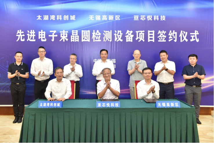
Jiwei.com reported recently, Jingsheng Electromechanical said in an institutional survey that the company has seized the industry trend of accelerating the localization of semiconductor equipment, accelerated the market verification and promotion of semiconductor equipment, and seized market share. The company's semiconductor equipment orders have achieved a rapid year-on-year increase. Growth; company actively develops photovoltaic innovations

to accelerate the expansion of production of advanced consumables, and actively promote the reduction of LCOE; strengthen the market development of photovoltaic equipment, further improve the quality of technical services, actively promote the delivery and acceptance of orders in hand, and achieve a substantial year-on-year increase in the scale of operating income and operating performance .

Jingsheng Electromechanical is a leading high-tech enterprise focusing on "advanced materials and advanced equipment" in China. It has developed a series of key equipment around the three major semiconductor materials of silicon, sapphire and silicon carbide, and has extended to the field of compound substrate materials.

In the field of silicon materials, the company has developed a series of key equipment used in the two major industries of photovoltaic and integrated circuits, including automatic crystal growth equipment, crystal processing equipment, wafer processing equipment, CVD equipment, shingled component equipment, etc.; in sapphire In the field of silicon carbide, the company can provide sapphire ingots, ingots and wafers that meet the needs of LED lighting substrate materials and window materials; in the field of silicon carbide, the company's products mainly include silicon carbide crystal growth, polishing, epitaxy equipment and 6-inch conductivity type Silicon carbide substrate.

At the same time, the company has also established a product system based on high-purity quartz crucibles, diamond wires, semiconductor valves, pipe fittings, magnetic fluids, and precision components, supporting key components required for semiconductor and photovoltaic equipment and core auxiliary components required by the industrial chain. meet the needs of materials and consumables; take the material production and processing equipment chain as the main line, realize the digital and intelligent connection between various equipment, and provide customers with solutions of lean manufacturing + digitization + AI big data; set up a professional technical service team, Set up service centers in areas where customers are concentrated to realize a full range of localized services of after-sales + accessories + technical services + personnel training, and maximize the value of customer equipment through industry-leading professional capabilities and services that exceed customer needs.

Jingsheng Electromechanical said that semiconductor equipment is mainly divided into three major links: silicon wafer manufacturing, chip manufacturing, and packaging manufacturing. The equipment produced by the company is mainly used for the growth and processing of semiconductor silicon wafers. It belongs to the silicon wafer manufacturing link equipment. Some process links are laid out to the chip manufacturing and packaging manufacturing ends. With the continuous transfer of the international production capacity of the integrated circuit industry to the mainland of my country, the construction of integrated circuit production lines in mainland China continues to expand, and major manufacturers have laid out expansion plans, but the localization rate of equipment is low. Due to factors such as service response, equipment cost performance, and policy support, domestic substitution of equipment is a long-term theme that domestic equipment manufacturers and wafer manufacturers have jointly promoted.


Please, Log in or Register to view URLs content!
 

european_guy

Junior Member
Registered Member

Han's Laser: SiC ingot laser slicer and SiC ultra-thin wafer laser slicer are undergoing mass production verification​


16589997823628.png

Han's Laser stated on the investor interactive platform that the company's SiC ingot laser slicer and SiC ultra-thin wafer laser slicer are being verified by customers for mass production. The QCB technology used in the two products can greatly increase the production capacity on the basis of the original traditional wire cutting. Taking the ingot of 2cm thickness to produce wafers with final thicknesses of 350um, 175um and 100um, as an example, the increase rate is 40%. , 120% and 270% capacity.


Please, Log in or Register to view URLs content!

Some more detail on this quite new and promising technology (it seems the first to use it was Disco just few years ago):

Please, Log in or Register to view URLs content!
 

gadgetcool5

Senior Member
Registered Member
But also consider back them most equipment, device and material was basically designed at hand, they didn't have supercomputers to simulate billions of raytraced rays to optimize the optics of lithography equipment or make complex Multiphysics simulations to study the flow of chemicals in plasma etching equipment or the EDA tools to simulate billions of transistors or even the CAD tools that we have today that REALLY cut time on development. So yes equipment was simpler back them but modern design tools are way better than in the past. For god sake even mask design was done by hand.

View attachment 94328

View attachment 94329
Sure but China's problem has never been the inability to do chip design given imported EDA tools.
 

olalavn

Senior Member
Registered Member
[China has conquered 600 km/h high-speed maglev technology: filling the gap between high-speed rail and aircraft] According to the High-Speed Rail Quartet, July 29, "The 13th Five-Year Plan "national key research and development plan advanced rail transit key project "600 kilometers per hour" "Major technology research of Maglev transportation system" has successfully surpassed through performance evaluation and acceptance in Qingdao. It marks that my country has basically mastered the full range of high-speed maglev engineering and technology, and has the potential to further promote high-speed
 
Status
Not open for further replies.
Top