Chinese semiconductor industry

Status
Not open for further replies.

hvpc

Junior Member
Registered Member
Getting a bit more technical wouldn't hurt anyone. There may be some operational technical differences because this is clearly marketed towards maskless lithography systems but this dudes look pretty capable of easily make Arf lasers for lithography scanners, they probably don't do it because there is not such market in Russia but China is a potential huge market for them if they put some effort into it.

View attachment 93498
@tokenanalyst,
I'm actually curious which maskless writer company this guy is working with. Most DUV maskless writer I'm aware of are with wavelength longer than iLine plus the KrF mask writer you shared. Earlier this year, I had seen a paper or news article that Nikon is working on their 248nm and 193nm maskless NGL system. I tried to research it but couldn't find any info on the web.

I thought Nikon was nuts when I read earlier this year they are working on 248nm & 193nm maskless writer. Now, hearing about a 193nm laser for a possible another 193nm maskless writer, piqued my interest. Couldn't figure out what people want with a 193nm maskless writer, did I miss anything?

multiple multi beam writer suppliers are still working on that technology. In R&D setting that would like to eliminate need or photomask, these multi-beam maskless writers serve this purpose with better resolution. In HVM, scanners serve this purpose. Where would 193nm maskless writer fit in? Your thoughts on this?
 

dingyibvs

Junior Member
Was the person teaching it any good? I've often found that can make a bigger difference than the intrinsic difficulty of the material.
It's hard to find professors who are good at teaching. I think part of the reason I did well in Logic and Microprocessors was that the professor was a very good teacher, and that's because he was actually a lecturer and not a professor. As I'm sure you know pretty well already, professors are hired for their research competency, not their ability to teach. That's an unfortunate system, I think. I wonder if it's possible for universities to use a different system, where professors work with lecturers instead of directly teaching students. It'd cost more, but I think both professors and students would love it.
 

BlackWindMnt

Captain
Registered Member
It's hard to find professors who are good at teaching. I think part of the reason I did well in Logic and Microprocessors was that the professor was a very good teacher, and that's because he was actually a lecturer and not a professor. As I'm sure you know pretty well already, professors are hired for their research competency, not their ability to teach. That's an unfortunate system, I think. I wonder if it's possible for universities to use a different system, where professors work with lecturers instead of directly teaching students. It'd cost more, but I think both professors and students would love it.
Teaching things is hard, like a complete separate skill set that comes mostly natural.
Especially now that i'm in a more senior position and sometimes have to help the more junior developers.
I can already tell from that experience i would be a bad teacher.

Teaching requires someone to know how to talk, know how to pick the correct words its almost like diplomacy wouldn't be surprised if a good diplomat would make a good teacher and a good teacher also has the potential to be a good diplomat.
 

tokenanalyst

Brigadier
Registered Member
I'm actually curious which maskless writer company this guy is working with. Most DUV maskless writer I'm aware of are with wavelength longer than iLine plus the KrF mask writer you shared. Earlier this year, I had seen a paper or news article that Nikon is working on their 248nm and 193nm maskless NGL system. I tried to research it but couldn't find any info on the web.
I really don't know, they seem that they are just selling the light source.
Also they claim that the energy stability of their system is above 2 sigma % or above of 97.7% stable.

hearing about a 193nm laser for a possible another 193nm maskless writer, piqued my interest. Couldn't figure out what people want with a 193nm maskless writer, did I miss anything?
Probably to make chips for the militarily, to find a balance between volume and better resolution, the throughput of a 193nm direct writing laser system will be slow but still faster than a e-beam system and it could be used to write down to the 100-90nm. the KrF system that i posted have a resolution of 200nm and throughput of 40mm2/min, that is a bit faster than an e-beam system, it could be as slow as 1mm2 every 4 min according to one study i found.

Also could be really expensive, the optics have to be good because 193nm wavelength is very energetic and could wear out the system. Even a 248nm is already pretty crazy.

I will check if can find some information about that Nikon system, sounds really interesting.
 

tokenanalyst

Brigadier
Registered Member
@tokenanalyst, do you know what is the application of this KrF maskless system you found? I looked at their website and can't really tell what the Ath3000M is for (for FE IC? for MEM?).
Looks like they marketed that system for mask fabrication but I guess also could be used for low volume fabrication of ICs and MEMs devices.
But looks like they are not active anymore.
 

tokenanalyst

Brigadier
Registered Member

TSMC Trims Expansion Plans as Outlook Dims.​


TSMC also said that the cost of building its new 5nm
Please, Log in or Register to view URLs content!
will be higher than expected.

“During these past two years, we found that the labor cost in the States is higher than we planned,” TSMC chairman Mark Liu said at the event. “Some of the Covid supply chain interruptions also were unexpected.”

“Our customers in the U.S. all want to load that fab,” he added. “We also believe there is ample business opportunity there. The cost is increasing, but cost is not the only factor. We are still working on government subsidies, and we’ll continue working on cost reduction.”

TSMC is counting on a
Please, Log in or Register to view URLs content!
from the U.S. government worth $52 billion that is aimed at reviving the American chip industry.


Please, Log in or Register to view URLs content!
 

tokenanalyst

Brigadier
Registered Member
Yeah about that:

"You have Intel that might get $20 billion with CHIPS Act plus $5 billion or $10 billion under the FABS Act," said an official for one unnamed Intel competitor that is opposed to the soon-to-be-voted upon version of the CHIPS and FABS Acts. "So, $30 billion goes to your direct competitor, and you don't get a penny? That's going to cause problems in the market."

Intel wants 57% of the subsidies from the Chips act, the rest of the money 22 billion will divided among other U.S. companies. TSMC will probably get nothing.
 

ansy1968

Brigadier
Registered Member
Yeah about that:

"You have Intel that might get $20 billion with CHIPS Act plus $5 billion or $10 billion under the FABS Act," said an official for one unnamed Intel competitor that is opposed to the soon-to-be-voted upon version of the CHIPS and FABS Acts. "So, $30 billion goes to your direct competitor, and you don't get a penny? That's going to cause problems in the market."

Intel wants 57% of the subsidies from the Chips act, the rest of the money 22 billion will divided among other U.S. companies. TSMC will probably get nothing.
@tokenanalyst Yeah Its suck to be a bastard child.
 

hvpc

Junior Member
Registered Member
Looks like they marketed that system for mask fabrication but I guess also could be used for low volume fabrication of ICs and MEMs devices.
But looks like they are not active anymore.
Ah. If it's a mask writer, the spec they published would make sense now.
I will check if can find some information about that Nikon system, sounds really interesting.
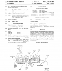
The patent you found is indeed the Digital Scanner that Nikon speaks of. Of the three applications that Nikon is pushing for, the first two (rapid prototyping, and design customization) are not new. The third application, large area printing, is a new novel idea to me. One large printing application is to address the stitching issue that comes with the use of multiple masks for interposers. This does sound interesting, but I wonder if the economic of it would make sense. I'll have to do some estimating and verify if the math (the ROI of this application) would work.

Nikon is targeting a KrF, ArF, and ArFi maskless digital scanners with throughput of 20wph. This is quite fast, and ambitious. For comparison purpose, that Ath300M KrF maskless system (40mm^2/min) would take >20hours to expose an entire 300mm wafer, Nikon is targeting 3minutes per wafer with their KrF digital scanner! I'm curious what price range they would target, this would definitely impact its adoption rate.
 
Status
Not open for further replies.
Top