Chinese semiconductor industry

Status
Not open for further replies.

tokenanalyst

Brigadier
Registered Member
Thanks. This means that domestic ion implanters are even more important than I thought. They used to be monopolized by US.
Yeah I agree and they are also very important in other areas like wide band-gap semiconductors like Silicon Carbide, Gallium Nitride (necessary for power applications like EV and 5G) and for the photovoltaic industry (There is were Kingstone and CETC started in ion implantation before jumping to IC fabrication).
Apart from lithography this is one the technologies that a country may need to develop if they don't want to be subject to other countries irrational will in this area.​
 

alfreddango

Junior Member
Registered Member
I have some questions that are tangentially related to semiconductors:

1) in
Please, Log in or Register to view URLs content!
it is said that high-end radio frequency (RF) components are monopolised by the usa; "U.S. companies Skyworks, Qorvo, and Broadcom “monopolize” the high-end market for the “key” RF component, the power amplifier chip (or RF chip). There are “essentially” no Chinese firms at all in the high-end RF chip market. U.S. manufacturers such as Qorvo “entirely” dominate the market for another class of RF components: high-end wave filters used in mobile phones.
if china improves its semiconductor industry, is this one of the sectors where over reliance on the usa could be lessened?

2) I think I read somewhere here on the forum that american aesa radars have qorvo chips in them. and I've learnt that chinese military aesa radars are very good quality. If point 1 is true, how did china manage to achieve such quality for aesa radars if they rely on american chips that are probably sanctioned by now? do chinese companies use home-grown" chips that are from bigger nodes but that the chinese semiconductor industry has already mastered?
 

latenlazy

Brigadier
Developing of SSMB technology will probably work in China and nowhere else....but once it will be industrialized and a commercial product is made out of it, I'd think this will be interesting and useful for everybody in the long term. Apparently SSMB allows easier scaling to shorter light wavelength beyond 13,5nm than current LPP solutions, so it seems a future-proof technology.
I did mention this in one of my posts but it’s not necessarily going to be the case that you can continue toward ever shorter wavelengths for process node shrinks. EUV already has issues with its photons being too high energy and thus causing all sorts of secondary issues with line accuracy from effects like shot noise and material ionization. Going to even shorter wavelengths just exacerbates those kinds of issues, and it may not be workable for ever smaller nodes since these effects ultimately impact effective resolution, especially given that there probably isn’t much room to shrink left.
 

FairAndUnbiased

Brigadier
Registered Member
I have some questions that are tangentially related to semiconductors:

1) in
Please, Log in or Register to view URLs content!
it is said that high-end radio frequency (RF) components are monopolised by the usa; "U.S. companies Skyworks, Qorvo, and Broadcom “monopolize” the high-end market for the “key” RF component, the power amplifier chip (or RF chip). There are “essentially” no Chinese firms at all in the high-end RF chip market. U.S. manufacturers such as Qorvo “entirely” dominate the market for another class of RF components: high-end wave filters used in mobile phones.
if china improves its semiconductor industry, is this one of the sectors where over reliance on the usa could be lessened?

2) I think I read somewhere here on the forum that american aesa radars have qorvo chips in them. and I've learnt that chinese military aesa radars are very good quality. If point 1 is true, how did china manage to achieve such quality for aesa radars if they rely on american chips that are probably sanctioned by now? do chinese companies use home-grown" chips that are from bigger nodes but that the chinese semiconductor industry has already mastered?
Uh the vast majority of RF power amplifiers are 2.5-5V low power (mW) devices for use in Bluetooth, Wifi, etc.

These are not used for radar. The volume of lower power RF amplifiers is extremely high (billions) compared to radar high power amplifiers (maybe 1 million at most). They have very different requirements. So there's no contradiction.

Please, Log in or Register to view URLs content!
 

latenlazy

Brigadier
I have some questions that are tangentially related to semiconductors:

1) in
Please, Log in or Register to view URLs content!
it is said that high-end radio frequency (RF) components are monopolised by the usa; "U.S. companies Skyworks, Qorvo, and Broadcom “monopolize” the high-end market for the “key” RF component, the power amplifier chip (or RF chip). There are “essentially” no Chinese firms at all in the high-end RF chip market. U.S. manufacturers such as Qorvo “entirely” dominate the market for another class of RF components: high-end wave filters used in mobile phones.
if china improves its semiconductor industry, is this one of the sectors where over reliance on the usa could be lessened?

2) I think I read somewhere here on the forum that american aesa radars have qorvo chips in them. and I've learnt that chinese military aesa radars are very good quality. If point 1 is true, how did china manage to achieve such quality for aesa radars if they rely on american chips that are probably sanctioned by now? do chinese companies use home-grown" chips that are from bigger nodes but that the chinese semiconductor industry has already mastered?
No RF chips, American or Chinese, use advanced nodes. Semiconductors for power electronics don’t follow the same performance parameter drivers that semiconductors for computing do.
 

tokenanalyst

Brigadier
Registered Member
I have some questions that are tangentially related to semiconductors:

1) in
Please, Log in or Register to view URLs content!
it is said that high-end radio frequency (RF) components are monopolised by the usa; "U.S. companies Skyworks, Qorvo, and Broadcom “monopolize” the high-end market for the “key” RF component, the power amplifier chip (or RF chip). There are “essentially” no Chinese firms at all in the high-end RF chip market. U.S. manufacturers such as Qorvo “entirely” dominate the market for another class of RF components: high-end wave filters used in mobile phones.
if china improves its semiconductor industry, is this one of the sectors where over reliance on the usa could be lessened?

2) I think I read somewhere here on the forum that american aesa radars have qorvo chips in them. and I've learnt that chinese military aesa radars are very good quality. If point 1 is true, how did china manage to achieve such quality for aesa radars if they rely on american chips that are probably sanctioned by now? do chinese companies use home-grown" chips that are from bigger nodes but that the chinese semiconductor industry has already mastered?
1- After the Huawei sanctions some Chinese companies are jumping in the bandwagon of RF ICs, even Hisilicon is jumping, in any case if the sanctions get worse this companies will try to fill the hole in domestic demand. So there is a lot of opportunity for growth.

Please, Log in or Register to view URLs content!

2- Military chips and civilian chips have different specifications, probably the qorvo chips used by U.S. radar are probably designed and fabbed to certain extend differently than civilians chips, in the case of China CETC is the one making this kind of military chips. The problem is that military chips are made without regard of price considerations because the military is willing to pay premium for their high end reliable chips, so any civilian application would probably require some big redesign to reduce costs.​
 

tokenanalyst

Brigadier
Registered Member
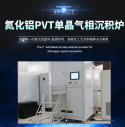
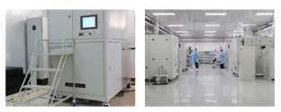
There are even companies developing the materials and the equipment needed to make the materials for this kind of chips.


1655846709453.png1655847142232.png

The core of Aoxiang Optoelectronics focuses on the third/fourth generation ultra-wide bandgap semiconductor aluminum nitride wafer substrate materials, sapphire-based/silicon-based/silicon carbide-based aluminum nitride/aluminum nitride scandium thin film templates, fully automatic nitrogen R&D, manufacturing and sales of aluminum chemical PVT vapor deposition furnaces and related products. The core products are included in the "Made in China 2025" key strategic new materials and equipment catalogue. It is an ideal substrate/piezoelectric material for various types of ultraviolet light-emitting devices such as electrical sensors, high-temperature/high-frequency radio-frequency devices, high-frequency/high-power electronic and laser devices.

After years of high-intensity R&D investment, Aoxiang Optoelectronics has successfully developed the world's largest aluminum nitride single crystal and wafer with a diameter of 60mm, and is also the world's first mass manufacturer of aluminum nitride thin film templates. Currently, we can provide customers with 1-inch/2-inch high-quality aluminum nitride single crystal substrates, 2/4/6-inch sapphire-based/silicon-based/silicon carbide-based aluminum nitride, aluminum nitride scandium thin film templates, aluminum nitride single crystal substrates At the same time, it provides customers and partners with complete process solutions from equipment design, thermal field design, thermal field simulation technology development, consultation and growth process optimization to wafer process. Professional technical services. As of April 2021, a total of 40 international and domestic patents have been applied for/authorized. It is one of the teams with the largest number of patents in this field in the world, and is recognized as a global technology leader in this field.​

Please, Log in or Register to view URLs content!
 

ansy1968

Brigadier
Registered Member
From our esteem member @Oldschool, seems like a Chinese EUVL is on the Horizon with SSMB, no question about it, collaborating the post of another esteem members @tokenanalyst , when? with research being done on optics and materials using SSRF, I'll say sooner with 2026/2027 as a conservative date.


Oldschool

Junior Member​

Registered Member
19 minutes agoNew
Shanghai has a synchrotron facility
Please, Log in or Register to view URLs content!


recently it posted 2 post doctoral research jobs relating to sub-7nm IC research application with synchrotron facility

Please, Log in or Register to view URLs content!

中国科学院上海高等研究院(下称高研院)坐落于上海市浦东新区张江科学城核心区,是一所年轻的多学科交叉的综合性科教机构。高研院主要以先进光源大科学装置的研制、建设和运行为核心,开展加速器科学、光子科学、能源科学与信息科学领域的原始创新研究和关键
Please, Log in or Register to view URLs content!


Shanghai Institutes for Advanced Study, Chinese Academy of Sciences will recruit 2 postdoctoral researchers in June 2022​

Source: Science Talent Network
Release time: 2022-06-15
Located in the core area of Zhangjiang Science City, Pudong New Area, Shanghai, the Shanghai Institutes for Advanced Study of the Chinese Academy of Sciences (hereinafter referred to as "Advanced Research Institute") is a young multidisciplinary comprehensive scientific and educational institution. The Advanced Research Institute mainly focuses on the development, construction and operation of advanced light source large scientific devices, carries out original innovation research and key core technology research and development in the fields of accelerator science, photon science, energy science and information science, supports cutting-edge scientific research, and provides core technologies And integrated technology solutions, responsible for the operation and opening of national large scientific infrastructure such as Shanghai Synchrotron Radiation Light Source and National Protein Facility (Shanghai).
Due to work needs, we are recruiting 2 postdoctoral researchers:
1. Recruitment requirements and conditions:
(1) Position 1 (1 person):
Research direction: synchrotron radiation research on two-dimensional material interfaces and energy information devices.
Participate in projects or topics after entering the station: synchrotron radiation characterization and application research of Sub-7nm advanced integrated circuit devices; research on dynamic electrochemical process of layered materials based on synchrotron radiation in situ X-ray spectroscopy technology; two-dimensional metal chalcogenide reversible storage Multidimensional in situ synchrotron radiation studies of potassium interface and structural properties, et al.
Work content:
1. Synchrotron radiation characterization and application of two-dimensional material structure interface;
2. Development of high spatiotemporal resolution synchrotron radiation characterization devices and technical methods for energy information material devices;
3. Research on the construction and mechanism of high-performance energy information devices based on two-dimensional materials;
4. Other work arranged by the instructor.
Admission requirements:
1. Support the party's line, principles and policies, love the motherland, abide by the law; have the scientific spirit of continuous innovation, abide by academic ethics and scientific research integrity, be honest and self-disciplined, have a decent style of study, and be of good character; the age should be under 35 years old, and a doctorate degree is generally accepted. not more than 3 years;
2. Doctorate degree in physics, energy information or related professional background;
3. Publish 3 or more SCI articles as the first author during Ph.D., at least one first-author article has an impact factor greater than 15, and the sum of the first-author article impact factor during Ph.D. is greater than 30 (the three requirements must be met at the same time);
4. The research background of two-dimensional energy material devices and synchrotron radiation is preferred.
(2) Position 2 (1 person):
Research Interests: Synchrotron X-ray Diffraction Characterization of Interfaces of Novel Mass Transfer and Communication Devices.
Participate in projects or topics after entering the station: development of high-throughput synchrotron radiation characterization technology for integrated circuit materials; research on electronic structure of magnetic topological materials; in-situ synchrotron radiation X-ray diffraction research on chemical vapor deposition doped/intercalated graphene structures.
Work content:
1. Synchrotron radiation solid-liquid, liquid-liquid mass transfer interface diffraction characterization device and technology development;
2. Synchrotron X-ray diffraction study on interface structure of new information and communication devices (optical communication, ion mass transfer).
Admission requirements:
1. Support the party's line, principles and policies, love the motherland, abide by the law; have the scientific spirit of continuous innovation, abide by academic ethics and scientific research integrity, be honest and self-disciplined, have a decent style of study, and be of good character; the age should be under 35 years old, and a doctorate degree is generally accepted. not more than 3 years;
2. Doctorate degree in physics, optical information or related professional background;
3. Publish 3 or more SCI articles as the first author during Ph.D., at least one first-author article has an impact factor greater than 15, and the sum of the first-author article impact factor during Ph.D. is greater than 30 (the three requirements must be met at the same time);
4. A background in research work related to synchrotron radiation X-ray diffraction is preferred.
2. Treatment:
In accordance with the relevant standards of the Shanghai Institute for Advanced Study.
3. Contact information:
Interested candidates please send your resume to the following contact information (please indicate "name + graduate school/work unit + postdoctoral application" in the subject of the email), while the number of applicants is full.
Contact: Mr. Zhu
Email: [email protected], CC [email protected]
Website:
Please, Log in or Register to view URLs content!

Address: No. 99, Haike Road, Zhangjiang Hi-Tech Park, Pudong, Shanghai
Postcode: 201210
The information comes from the Internet. If there is any change, please refer to the original publisher.
Source link:
Please, Log in or Register to view URLs content!


Please, Log in or Register to view URLs content!

中科院上海高研院征才,依托上海光源大科学装置,发力7纳米以下节点先进集成电路研发。
laoyaoba.com
laoyaoba.com


An add on from @tokenanalyst previous post

Shanghai Institute of Advanced Research, Chinese Academy of Sciences recruits talents to develop advanced integrated circuits with nodes below 7 nanometers​

Please, Log in or Register to view URLs content!

2589
set microgrid

Source: Aijiwei
#photoresist#
#Shanghai Light Source#
node-media-time.png

17 hours ago
16557959706703.png


According to the news of Micronet, the Shanghai Institutes for Advanced Study of the Chinese Academy of Sciences recently released a post-doctoral researcher recruitment notice. After entering the station, the candidates will participate in the synchrotron radiation characterization and application research of Sub-7nm advanced integrated circuit devices.

According to public information, "Synchronous Radiation Characterization Technology and Application for Sub-7nm Advanced Process Node Integrated Circuit Core Devices" is the 2021 project of the national key research and development plan "Frontier Research on Large Scientific Devices", led by Shanghai Advanced Research Institute, and the project is implemented. With a cycle of 5 years, this job posting may show that the R&D project has been substantially started.

According to information from Nankai University, Luo Feng, a chair professor of the school, has also undertaken corresponding topics and carried out photoresist synthesis and etching evaluation of extreme ultraviolet lithography technology. The company's partners include SMIC's Northern Integrated Circuit Innovation Center and Beijing Superstring Memory Research Institute. (Proofreading/Aileen)
 
Status
Not open for further replies.
Top