Chinese semiconductor industry

Status
Not open for further replies.

tokenanalyst

Brigadier
Registered Member

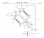
A device and method for generating target droplets of euv light source​

Abstract

Zhejiang University ZJU (A first)​

CN112286011B​

2021

The present invention relates to a EUV light source target droplet generating device and method. The droplet generating assembly, droplet separation assembly and liquid recovery assembly of the present invention; the droplet generating assembly includes a storage tank, a cavity, a heating device, a pressure source, an excitation module, a disturbance rod and a micro-hole nozzle; the droplet separation assembly includes a belt Orifice electrode plate and deflection electrode plate; liquid recovery assembly including liquid collector. The invention utilizes the principle of Rayleigh instability to generate droplets, and sorts droplets of appropriate size as EUV The target droplet bombarded by the laser light source system of the lithography machine. The target droplet of extremely small size can be obtained, which improves the energy conversion efficiency of laser bombardment of the target droplet; the jet nozzle with a larger size can be used to reduce the manufacturing cost; the target droplet material is recycled and reused to improve the use efficiency and reduce the cost.​

1654026351571.png
 

gelgoog

Brigadier
Registered Member
Semiconductor industry analysts said the semiconductor technology gap between South Korea and China grew by around three years thanks to US controls on exports to China dating back to the Trump administration
Please, Log in or Register to view URLs content!
This is to be expected, at least in the short term. For example, the major DRAM manufacturers are moving to using EUV now, while Chinese DRAM makers such as CXMT will be stuck at 1x nm or 1y nm level for a while. But it's important for China to stick to the strategic goal of removing bottlenecks and achieve self-sufficiency in key parts of the supply chain, after which China will control its own pace and destiny.
Samsung is in deep poo poo because of their yields scam. They lost NVIDIA and a lot of their other customers have been jumping ship as well. Samsung cannot deliver logic chips in the advanced processes with the required volumes.

Samsung's memory division is doing great. Samsung recently released the spec for UFS 4.0 and they are supposed to be mass producing a product with that in Q3. Also supposed to ship a 200+-layer product in late this year and currently mass producing 176-layer NAND.

YMTC has been steadily advancing on their roadmap and they have put their 4th generation 192-layer 3D NAND into sample production. They also recently released their product with UFS 3.1 and you have mentions of them working on their own memory controller design. So I would say YMTC is at most like a year behind Samsung, the market leader, in VNAND. If not like 6 months. What YMTC needs I think is to increase their production.

CXMT is still producing LPDDR4 products and hasn't shipped a LPDDR5 product yet. In the long term CXMT cannot compete properly with the other DRAM memory vendors because they are stuck using DUV when everyone else either is already using or switching to adding EUV to their production lines. They need to come up with a 3D structure similar to what was done to VNAND I think.

YMTC can continue scaling if they establish a good relationship with Chinese companies which make etching devices and continue improving on their technology. But CXMT in the long run is stuck unless they come up with a new cell architecture not used in the industry yet.
 

coolieno99

Junior Member
The dudes from Tsinghua got a WIPO patent on their SSMB EUV light source.

Electron beam storage ring and extreme ultraviolet light source with the electron beam storage ring​

Abstract​

An electron beam cluster storage ring (100), the electron beam cluster storage ring (100) comprises a plurality of deflection structures (110) and a plurality of linear segments (120) connecting the deflection structures (110), the deflection structures (110) and the linear segments ( 120) together form a ring-shaped structure suitable for the continuous running of the electron beam cluster, and in the running direction of the electron beam, each deflection structure (110) is sequentially arranged with a front end matching section (116), a front end matching unit (118), continuous with each other; A number of main units (112), a rear end matching unit (119) and a rear end matching section (122) are arranged, and the magnets in the electron bunch storage ring (100) are appropriately arranged so that the magnets outside the matching unit (114) The integral values of the dispersion functions in all the diodes (B1, Bm) are zero, and the dispersion functions and their derivatives at the entrance of the front-end matching unit (118) and the exit of the back-end matching unit (119) are zero, In addition, the derivative value of the dispersion function at the junction of the diodes (B1, Bm) of the adjacent main units (112) is zero.

Description​

Electron beam storage ring and extreme ultraviolet light source with the electron beam storage ring technical field
The present invention relates to a storage ring for storing ultrashort electron beam clusters (eg beam length 100 nm). The present invention also relates to a steady-state microbunching-based extreme ultraviolet (UV) with such a storage ring EUV light source, the extreme ultraviolet light source is used to generate ultra-high power extreme ultraviolet laser, especially suitable for nano chip lithography applications and other fields.

View attachment 89815
The advantages of SSMB EV light source over LPP EUV light source are:
1. 4 times the light power output
2 Non-contanimation of main mirror by tin atoms

Please, Log in or Register to view URLs content!
 

tinrobert

Junior Member
Registered Member
How about provide us with the bidding list so everyone can see what data you reference?

The existence of second hand 28 nm suitable equipment means that new ones have lower demand. Lower process requirements means more equipment is suitable. This is very simple logic.

Deciding what node to build depends primarily on customer demand at SMIC. Itis very academic for you to say only highest node should be built but what's the business case? Of 28 nm + FinFET how much is 28 nm, how much is FinFET? You don't know, I don't either.

The demand at SMIC doesn't necessarily match the demand of the market as a whole. How come nobody says Texas Instruments is a stone age company because they don't even have a single FinFET fab? Exactly.

Please, Log in or Register to view URLs content!

How come Texas Instruments is focusing on 45 nm fab? They have 28 nm products but focus on 45 nm fab. I guess by your logic it must be because their 28 nm process is shit and useless, not because they have a better business case for 45 nm and more demand at 45 nm.
Sometimes it's the geometry or type of chip. For example, a 180nm micron SiGe BiCMOS process is able to achieve speeds comparable to a 90 nanometer RF CMOS process. As a result, SiGe BiCMOS makes it possible to create analog products using a larger geometry process technology at a lower cost while achieving similar or superior performance to that achieved using a smaller geometry standard RF CMOS process technology.
 

tinrobert

Junior Member
Registered Member
Samsung is in deep poo poo because of their yields scam. They lost NVIDIA and a lot of their other customers have been jumping ship as well. Samsung cannot deliver logic chips in the advanced processes with the required volumes.

Samsung's memory division is doing great. Samsung recently released the spec for UFS 4.0 and they are supposed to be mass producing a product with that in Q3. Also supposed to ship a 200+-layer product in late this year and currently mass producing 176-layer NAND.

YMTC has been steadily advancing on their roadmap and they have put their 4th generation 192-layer 3D NAND into sample production. They also recently released their product with UFS 3.1 and you have mentions of them working on their own memory controller design. So I would say YMTC is at most like a year behind Samsung, the market leader, in VNAND. If not like 6 months. What YMTC needs I think is to increase their production.

CXMT is still producing LPDDR4 products and hasn't shipped a LPDDR5 product yet. In the long term CXMT cannot compete properly with the other DRAM memory vendors because they are stuck using DUV when everyone else either is already using or switching to adding EUV to their production lines. They need to come up with a 3D structure similar to what was done to VNAND I think.

YMTC can continue scaling if they establish a good relationship with Chinese companies which make etching devices and continue improving on their technology. But CXMT in the long run is stuck unless they come up with a new cell architecture not used in the industry yet.
True for CXMT. But remember Micron is still using DUV and wont be using EUV until its 1-gamma chip. The 1-alpha is in production now, the 1-beta next year, the 1-gamma year after. It is installing EUV at Taichung fab this year.
 

european_guy

Junior Member
Registered Member
@european_guy bro what about CETC? the excitement and joy of being a Chinese Semiconductor watcher, you don't know what you gonna get. Plus Ignore it at your owned peril...lol

Please, Log in or Register to view URLs content!

Please, Log in or Register to view URLs content!


Mar 17, 2021 — The ion implanters are all made in China and can provide a one-stop service for global chipmakers, the CETC added.

Thanks! You are right there is also CETC.

Please, Log in or Register to view URLs content!
 

european_guy

Junior Member
Registered Member
Semiconductor industry analysts said the semiconductor technology gap between South Korea and China grew by around three years thanks to US controls on exports to China dating back to the Trump administration
Please, Log in or Register to view URLs content!

They write:

"Semiconductor industry analysts said the semiconductor technology gap between South Korea and China grew by around three years thanks to US controls on exports to China dating back to the Trump administration."

This is a very superficial statement. It is completely different to be, say many years behind in advanced IC chips, and also even more or not existent in large parts of semiconductor supply chain (like China was few years ago), and be say even 3 years more in delay in advanced IC chips, but only due to a single equipment (EUV litho machine), while you have fully localized almost all the rest, like China will be in few years from now.

For 2025, apart from EUV (and EDA tools), everything else will be localized. At that point the "advantage" of US bloc, will be very fragile.

Of course US is trying to cut out China from semiconductor supply chain and semi equipment market, so they need to "convince" Japan, Holland and Korea (in order of increasing difficulty).
 

european_guy

Junior Member
Registered Member
In April 2022, domestic equipment manufacturers won 26/36 etching equipment bidding.

Please, Log in or Register to view URLs content!

"In April 2022, the number of etching equipment in mainland China was 36, and the number of domestic equipment manufacturers was 26, including 14 from North Huachuang and 12 from China Micro."

The only other supplier that won 12 machines is TEL (Tokyo Electron): Us firms AMAT and Lam Research are out. I guess this is very telling. Currently they make 30% of their revenue from China market.....big clouds linger on their horizon.
 

ansy1968

Brigadier
Registered Member
They write:

"Semiconductor industry analysts said the semiconductor technology gap between South Korea and China grew by around three years thanks to US controls on exports to China dating back to the Trump administration."

This is a very superficial statement. It is completely different to be, say many years behind in advanced IC chips, and also even more or not existent in large parts of semiconductor supply chain (like China was few years ago), and be say even 3 years more in delay in advanced IC chips, but only due to a single equipment (EUV litho machine), while you have fully localized almost all the rest, like China will be in few years from now.

For 2025, apart from EUV (and EDA tools), everything else will be localized. At that point the "advantage" of US bloc, will be very fragile.

Of course US is trying to cut out China from semiconductor supply chain and semi equipment market, so they need to "convince" Japan, Holland and Korea (in order of increasing difficulty).
@european_guy bro sad to say Europe is compromise and her recent action against Russia open a lot of eyes from Chinese tech industry, I mean cancelling the whole country as in every individual. What Canada had done to Meng Wanzhou is small compare to what happen to Russian Oligarch, confiscating their wealth thru extra ordinary means without due process. And I completely agree, the ship had sailed, the Chinese had long memories, with this sudden push by the US for new restriction, we may not wait for 2025 to see progress in all field.
 
Status
Not open for further replies.
Top