Chinese semiconductor industry

Status
Not open for further replies.

FairAndUnbiased

Brigadier
Registered Member
Advanced packaging tool performance will be improved but still not state of the art.

For example, backend steppers resolution has been in the 1um / 2um range whereas frontend scanner resolution is now at 13.5nm and moving even lower. Even the frontend iline scanners/steppers has resolution limit of 0.28um (280nm).

Going into heterogeneous integration, backend lithography tool will have to move into the gap that previously separated frontend and backend litho. The 2.5D/3D steppers from SMEE will be redefined to provide improved resolution down to 0.5um.

So, yes, backend tools are expected to have improved performance, but again, it's still not state-of-the-art compared to frontend tools. We'll be mostly implementing or porting known features or methods learned from frontend to backend.

Like I said earlier, since advanced packaging will be dealing in a larger physical size range (on a "um" scale), we could afford much much larger error tolerance, so hence not difficult at all (relative to the technology we have to come up with on a "nm" scale in the FE).

P.S. state-of-the-art = higher price tag. you can clearly see the difference in the level of technology by looking at the big price delta between FE & BE equipments. And new BE tool may be state-of-the-art versus older BE tool, but compared to older FE tools, it's still not very "state-of-the-art". It's all relative. right?
backend tools have requirements for large exposure field, so the relative overlay error still needs to be small and the optical systems will need to be different than frontend tools.

chip packaging has different requirements. porting front end tools won't work that well and specialized tools will need to be developed. another example is TSV. etch for TSV is very different than standard etches due to the very high aspect ratio required.
 

hvpc

Junior Member
Registered Member
backend tools have requirements for large exposure field, so the relative overlay error still needs to be small and the optical systems will need to be different than frontend tools.

chip packaging has different requirements. porting front end tools won't work that well and specialized tools will need to be developed. another example is TSV. etch for TSV is very different than standard etches due to the very high aspect ratio required.
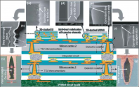
Again, if it needs the level of accuracy of FE iline scanners, our industry would've simply take a FE 4x iline scanner and put in a 2x reduction lens and be done with. But why wasn't this done? smaller "nm" come at higher tool price, which wouldn't be ideal for even advanced packaging litho tool. The biggest challenge of advanced packaging is trying to keep the cost under control and closer to the traditional packaging.

TSV HAR etch is still not as difficult. Look at price delta between TSV etcher and CCP/ICP etcher. Yes, HAR not easy, but DRAM capacitor is also relatively high aspect ratio (not as high as TSV) but much smaller in size and much denser. Different challenge, but again, difficulty is rewarded with higher tool price. The price is supporting evidence of the degree of difficulty.
TSV ~5um
DRAM storage node: <40nm now

As "advanced" as packaging go, it's still operates in a completely different physical size range. Here's a visual to show TSV vs. HAR DRAM capacitors (which you can't even see on the stack of DRAM chips on top because it's too small). The $ spent on FE vs BE is also very telling in which is more complex. Again, I'm not bashing and saying BE flow is not difficult or challenging, I'm just saying it's less so compared to the amount of work/innovation required to meet FE requirements.
1651478884635.png


1651478597786.png
 

virsuvei

Just Hatched
Registered Member
Please, Log in or Register to view URLs content!


What the heck is that all about? That ain't right.

India stealing money from Chinese companies!
It has been happening for ever. Nokia's Indian factory for mobile phones met big trouble when Indian authorities refused to follow the taxation treaties done between India and Finland. The factory had to be excluded from the deal when phone business was sold to Microsoft. Car makers like Ford and GM have exited India, so has Harley Davidson.
 

xypher

Senior Member
Registered Member
It has been happening for ever. Nokia's Indian factory for mobile phones met big trouble when Indian authorities refused to follow the taxation treaties done between India and Finland. The factory had to be excluded from the deal when phone business was sold to Microsoft. Car makers like Ford and GM have exited India, so has Harley Davidson.
Jai Hind
 

mrandolph

New Member
Registered Member
Great thread!

What is currently the most advanced chip, that can be bought either directly or inside a product, that is purely Chinese, in the sense that it is designed with open source or Chinese design software and produced with Chinese equipment or equipment that is outside the reach of American sanction power?

At one point there was internet chatter about a HiSilicon display driver chip made using a local 28nm process.

Anyone know the status of this?
 
Status
Not open for further replies.
Top