@european_guy So Bro what about the Shanghai Synchroton Facility? A vanity project? or a scientific /research center, from @WTAN, SMIC, ICRD, SMEE and others used it to research EUVL materials and component so that when the Beijing HEPS ( ) The fourth synchrotron to be built in China is operational, it can literally start producing chips as the components and materials had already been tested and maybe verify.If I remember correctly what I read here, the first SSMB underground facility will be ready for 2024/2025 and it will be mainly a scientific / technological project to make the SSMB concept to work in practice. From that you can expext at least some more years to make it viable in production, and so we are already toward 2030. I have no idea regarding plasma version, at the moment there is not even a prototype. Then there are tons of other issues like resists, masks, etc. that are still to be solved. Finally SMEE currently does not seem to be in mass production even with the non-immersion version of DUV and also its main suppliers are well behind (U-Precision will be ready in 2023, not clear about optical system, etc..).
Considering all the above, I can assume that by 2025, SMEE could be in mass production with immersion DUV (this is not a bad prediction, actually it is very optimistic one). And by the end of the decade toward 2028-2030 there will be a working prototype of EUVL machine, including needed localization of accessories like resist, masks, etc... Also this latter one is a very optimistic forecast, IMO.
You are using an out of date browser. It may not display this or other websites correctly.
You should upgrade or use an alternative browser.
You should upgrade or use an alternative browser.
Chinese semiconductor industry
- Thread starter Hendrik_2000
- Start date
- Status
- Not open for further replies.
That's irrelevant. These things take a long time to happen and given the importance of it, we shouldn't expect to have updates about it until the EUV has been developed and delivered to its first customerThe Huawei sanctions started like 3 years ago and we still don't have immersion lithography
I expect it by 2025And you expect EUV in 5 years?
I'm going blue in the face repeating myself, but here goes: Who. Says?No way. That is not how the industry operates.
Who said it takes 3 years and even if it did, who said it would take China 3 years? For the record, I never claimed "mass production" - I said that China would have a first-generation commercial EUV lithography machine in 2025. I actually didn't say it, @WTAN said it, and everything since his last post on page 1171 can get thrown in the trash can. He's the only one here who can so much as sniff a primary source. All the other claims and "analysis" in this thread is worthless.To have it in mass production in 3 years it would have to be in test fabs producing chips at a low rate RIGHT NOW.
No idea, but just because they're not sending me weekly updates like you seem to expect doesn't mean things aren't on track. Have you considered the possibility that China is developing this technology with some degree of secrecy?So where is it? Where is the EUV test line and facility?
@european_guy So Bro what about the Shanghai Synchroton Facility? A vanity project? or a scientific /research center, from @WTAN, SMIC, ICRD, SMEE and others used it to research EUVL materials and component so that when the Beijing HEPS ( ) The fourth synchrotron to be built in China is operational, it can literally start producing chips as the components and materials had already been tested and maybe verify.
From Beijing HEPS page:
"HEPS provides a state-of-the-art and multi-disciplinary experimental platform for basic science researchers"
This installation will be mainly a scientific / R&D project. I have never read that the target is to put this facility "in production" as light source for lithography. We can expect that, thanks to this very advanced facility, SSMB phenomenon will be fully characterized and a following, possibly smaller and simpler synchrotron facility aimed at lithography will be built using the knowledge gained at Beijing HEPS. So again, we are toward the end of the decade.
I will repost a Chinese Publication Highlighting China achievement in EUVL, 2 of the 3 core we had already mastered 1) the linear Lloyd lens coating device and nano-focusing lens coating device developed by Zhongke Kemei have also been put into use. 2) Huazhuo Precision Technology took the lead and independently developed a dual-stage system, one of the core technologies of EUV. Only the light source with DPP is a failure and here SSMB is crucial. So in a sense using the Shanghai Synchroton to research as a light source will make it easier the transition of using Beijing HEPS to power those FABS.
Chip manufacturing has always been the biggest shortcoming of the domestic semiconductor industry, and most of the chips we use, about 50% are purchased from the United States at high prices. According to statistics, from 2019 to 2020, Chinese chips The total amount of imports exceeds 300 billion, accounting for about 40% of the global semiconductor consumer market, far exceeding oil!
However, the old American, who has made a lot of money from the Chinese market, hates the rise of domestic high-tech companies such as Huawei. Industrial channels have caused Huawei HiSkong to have top-notch chip design skills, but it is useless.
The reason why we are trapped in the chip ban is largely due to the lack of EUV lithography equipment. However, ASML, the only Dutch giant that can produce EUV equipment in the world, is restricted by "export control" due to the American technology accessories contained in its production line, so that it has never been able to sell the equipment to us.
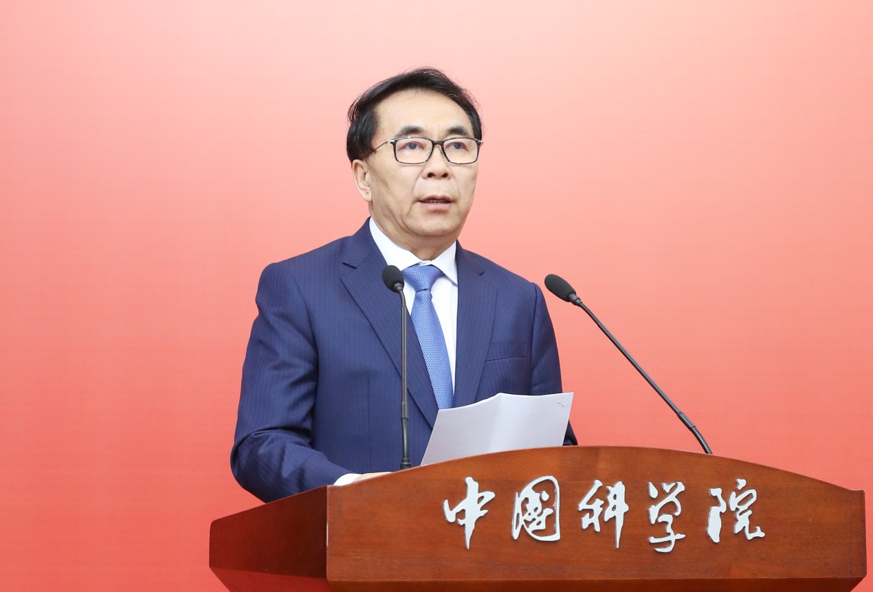
After Huawei was cut off, Ren Zhengfei visited the Chinese Academy of Sciences for help. The two sides reached a clear consensus: The key to breaking the ice of domestic chips is the EUV lithography machine.
In order to realize the rise of "China Core", the Chinese Academy of Sciences took the initiative to take over the task and established a special EUV core technology research team, which is bound to complete the breakthrough in the shortest time.
Unexpectedly, when ASML learned that we were going to develop EUV on our own, they would sneer and say: Even if they give Chinese drawings, they will make them. Although engineering academician Wu Hanming also said: EUV is the crystallization of global wisdom, it is very unrealistic for us to research and develop on our own.
However, in the face of Lao Mei's bottom-line suppression, we who are "stucked" have no room to "retire" at all. More importantly, the development of EUV is not only to clear the obstacles on the road to localization of chips, but also to safeguard the dignity of the nation!
Therefore, any doubts and ridicules cannot obliterate the determination of Chinese scientists to break through the EUV monopoly.
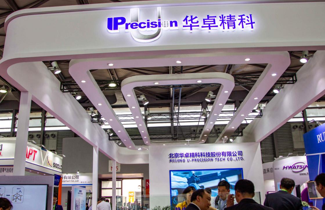
Sure enough, the good news came soon. Huazhuo Precision Technology took the lead and independently developed a dual-stage system, one of the core technologies of EUV, and became the second company in the world to master this technology after ASML.
Witnessing China's R&D progress in the field of lithography, ASML, which once poured cold water, also immediately changed its tune. Not only did it show its favor to the Chinese market five times, it even began to “snatch”, saying: If the United States continues sanctions, China will be alone within 15 years. Created EUV lithography machine.
However, ASML obviously still underestimated the perseverance and strength of Chinese scientists, and never expected it to be so fast. In just one year, China's EUV lithography machine was about to land.
In addition to the dual work stage system, EUV equipment has two core technologies, namely the light source and the optical lens.
In terms of light sources, the scientific research team led by Professor Tang Chuanxiang of Tsinghua University successfully explored a new type of particle accelerator light source "steady-state micro-bunching" in February this year. Ultraviolet light is the working light source of EUV. What's more commendable is that China's independent light source technology is not only suitable for EUV, but also has a wider range of application scenarios.
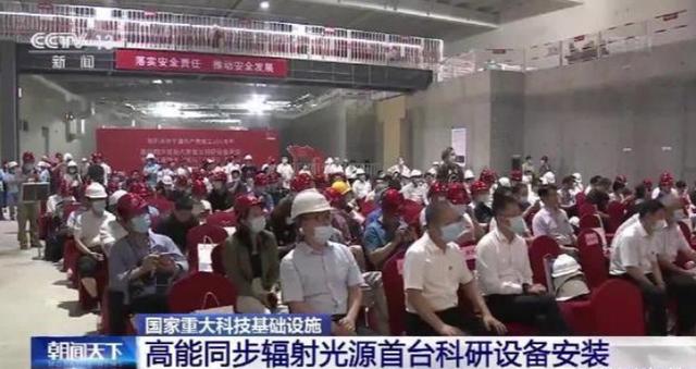
Only less than 6 months later, CCTV reported great news related to optical lenses.
The first domestic high-energy radiation light source equipment independently developed by the Chinese Academy of Sciences has officially completed the installation and application.
At the same time, the linear Lloyd lens coating device and nano-focusing lens coating device developed by Zhongke Kemei have also been put into use.
These two devices combined with high-radiation light source equipment can almost meet the physical lens technology of all process requirements, including Zeiss lenses.
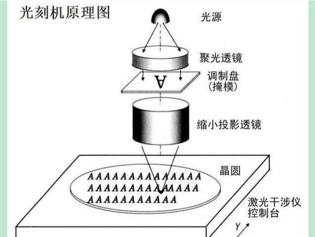
This means that the three core technologies of EUV lithography machines have all been broken, and the Chinese Academy of Sciences has also fulfilled its promise.
Although EUV claims to have more than 100,000 precision parts, it has not yet broken through, but can it be more aircraft carriers? This is not a big problem for the huge Chinese manufacturing market.
Looking back over the past seventy years, under the blockade of the West, China's scientific and technological development road has been very bumpy, but it has never stopped. One by one, the first achievements are coming. One super project has won the world, and scientific breakthroughs have benefited mankind. "Turning in circles, competing with hundreds of rivers" is the most appropriate description of China's science and technology. What is the point of a small EUV lithography machine?
EUV lithography machine announced a breakthrough, Chinese Academy of Sciences fulfilled its promise, ASML did not expect it to be so fast
2022-04-28 21:56 HKTChip manufacturing has always been the biggest shortcoming of the domestic semiconductor industry, and most of the chips we use, about 50% are purchased from the United States at high prices. According to statistics, from 2019 to 2020, Chinese chips The total amount of imports exceeds 300 billion, accounting for about 40% of the global semiconductor consumer market, far exceeding oil!
However, the old American, who has made a lot of money from the Chinese market, hates the rise of domestic high-tech companies such as Huawei. Industrial channels have caused Huawei HiSkong to have top-notch chip design skills, but it is useless.
The reason why we are trapped in the chip ban is largely due to the lack of EUV lithography equipment. However, ASML, the only Dutch giant that can produce EUV equipment in the world, is restricted by "export control" due to the American technology accessories contained in its production line, so that it has never been able to sell the equipment to us.

After Huawei was cut off, Ren Zhengfei visited the Chinese Academy of Sciences for help. The two sides reached a clear consensus: The key to breaking the ice of domestic chips is the EUV lithography machine.
In order to realize the rise of "China Core", the Chinese Academy of Sciences took the initiative to take over the task and established a special EUV core technology research team, which is bound to complete the breakthrough in the shortest time.
Unexpectedly, when ASML learned that we were going to develop EUV on our own, they would sneer and say: Even if they give Chinese drawings, they will make them. Although engineering academician Wu Hanming also said: EUV is the crystallization of global wisdom, it is very unrealistic for us to research and develop on our own.
However, in the face of Lao Mei's bottom-line suppression, we who are "stucked" have no room to "retire" at all. More importantly, the development of EUV is not only to clear the obstacles on the road to localization of chips, but also to safeguard the dignity of the nation!
Therefore, any doubts and ridicules cannot obliterate the determination of Chinese scientists to break through the EUV monopoly.

Sure enough, the good news came soon. Huazhuo Precision Technology took the lead and independently developed a dual-stage system, one of the core technologies of EUV, and became the second company in the world to master this technology after ASML.
Witnessing China's R&D progress in the field of lithography, ASML, which once poured cold water, also immediately changed its tune. Not only did it show its favor to the Chinese market five times, it even began to “snatch”, saying: If the United States continues sanctions, China will be alone within 15 years. Created EUV lithography machine.
However, ASML obviously still underestimated the perseverance and strength of Chinese scientists, and never expected it to be so fast. In just one year, China's EUV lithography machine was about to land.
In addition to the dual work stage system, EUV equipment has two core technologies, namely the light source and the optical lens.
In terms of light sources, the scientific research team led by Professor Tang Chuanxiang of Tsinghua University successfully explored a new type of particle accelerator light source "steady-state micro-bunching" in February this year. Ultraviolet light is the working light source of EUV. What's more commendable is that China's independent light source technology is not only suitable for EUV, but also has a wider range of application scenarios.

Only less than 6 months later, CCTV reported great news related to optical lenses.
The first domestic high-energy radiation light source equipment independently developed by the Chinese Academy of Sciences has officially completed the installation and application.
At the same time, the linear Lloyd lens coating device and nano-focusing lens coating device developed by Zhongke Kemei have also been put into use.
These two devices combined with high-radiation light source equipment can almost meet the physical lens technology of all process requirements, including Zeiss lenses.

This means that the three core technologies of EUV lithography machines have all been broken, and the Chinese Academy of Sciences has also fulfilled its promise.
Although EUV claims to have more than 100,000 precision parts, it has not yet broken through, but can it be more aircraft carriers? This is not a big problem for the huge Chinese manufacturing market.
Looking back over the past seventy years, under the blockade of the West, China's scientific and technological development road has been very bumpy, but it has never stopped. One by one, the first achievements are coming. One super project has won the world, and scientific breakthroughs have benefited mankind. "Turning in circles, competing with hundreds of rivers" is the most appropriate description of China's science and technology. What is the point of a small EUV lithography machine?
For I been seeing, optical sub-systems are expected to be mass produced in 2023 by Beijing e-town , U-Precision will probably produce their maglev 2.5nm wafer stage (which the say can be used for EUV) next year, Immersion sub-systems and parts are being mass produced by CHEERTECH, Photoresist for immersion is already been mass produced ,metrology e-beam sub-systems has been developed, lithography software has already been develop for both optical lithography and reflective optics. Mask for EUV is been develop and so is photoresist for EUV. Coating system for mass production of multilayer mirrors are been developed and so on. From my point of view the effort for the mass production of patterning systems (not just projective lithography but also nanoimprint and other forms of maskless lithography) in China is huge, is not just SMEE as some people say, is a nation wide effort that involves a lot of funds, companies and universities inside China. Personally I think people are underestimating how serious the Chinese are with this.If I remember correctly what I read here, the first SSMB underground facility will be ready for 2024/2025 and it will be mainly a scientific / technological project to make the SSMB concept to work in practice. From that you can expext at least some more years to make it viable in production, and so we are already toward 2030. I have no idea regarding plasma version, at the moment there is not even a prototype. Then there are tons of other issues like resists, masks, etc. that are still to be solved. Finally SMEE currently does not seem to be in mass production even with the non-immersion version of DUV and also its main suppliers are well behind (U-Precision will be ready in 2023, not clear about optical system, etc..).
Considering all the above, I can assume that by 2025, SMEE could be in mass production with immersion DUV (this is not a bad prediction, actually it is very optimistic one). And by the end of the decade toward 2028-2030 there will be a working prototype of EUVL machine, including needed localization of accessories like resist, masks, etc... Also this latter one is a very optimistic forecast, IMO.
To @hvpc and @european_guy here is my post dated Oct 20, 2020, and a link from @WTAN about a certain Chinese poster A-SET depicting about SSA800 and a possible EUVL. So to support my post that all the ingredients for a Chinese EUVL is there except for the power sources as the DPP lack power to make it commercially viable.
From WTAN previous post, please read the attach article, its very revealing and we can have a discussion.
02 Special Project is State project under 5 year plan 2016-2020 to create an advanced DUV Lithography machine by SMEE.
This new machine by SMEE model number is SSA800 and will be capable of making Chips in the 7nm node.
Note that Jiangsu Nata is also known as Nanda in the article by A-Set about 193nm Photoresist.
Article also says EUV machine will be available within 2 years. Maybe 2021 launch?
https://www.sinodefenceforum.com/attachments/image1-png.59648/
From WTAN previous post, please read the attach article, its very revealing and we can have a discussion.
I believe this is official media confirmation of the existence of the "02 Special Project".
02 Special Project is State project under 5 year plan 2016-2020 to create an advanced DUV Lithography machine by SMEE.
This new machine by SMEE model number is SSA800 and will be capable of making Chips in the 7nm node.
Note that Jiangsu Nata is also known as Nanda in the article by A-Set about 193nm Photoresist.
Article also says EUV machine will be available within 2 years. Maybe 2021 launch?
https://www.sinodefenceforum.com/attachments/image1-png.59648/
China-based semiconductor equipment suppliers see booming orders

Credit: DIGITIMES
Like its international peers, China-based semiconductor equipment maker Advanced Micro-Fabrication Equipment (AMEC) has had its delivery lead times prolonged due to components shortages, according to Chinese media reports.
@hvpc and here bro, The critics of SMEE DUVL use NXT 2000i as a bench mark thus the failure BUT the Chinese themselves use NXT1980i since at that time 2016 they have a unit to study and learn to create a comparable unit. And since all ASML DUVL had the same MMO of 2.5nm, The SSA800 can be improved upon with an iteration and reach the level of NXT 2050i, the SSA 900 22nm DUVL.
SMIC Chengdu foundry, using Shanghai microlithography machine SSA800/10W immersion lithography machine Parameters: Lens NA: 1.35 Single exposure resolution: 38-41nm Double workpiece table: DWSi, the productivity is 200 wafers per hour Round overlay accuracy: better than 2.5nm Design index: able to meet the process requirements of 28nm planar planner transistor logic circuit under single exposure conditions
SMIC Chengdu foundry, using Shanghai microlithography machine SSA800/10W immersion lithography machine Parameters: Lens NA: 1.35 Single exposure resolution: 38-41nm Double workpiece table: DWSi, the productivity is 200 wafers per hour Round overlay accuracy: better than 2.5nm Design index: able to meet the process requirements of 28nm planar planner transistor logic circuit under single exposure conditions
• 8 months ago • 8 months ago • Favorites •SMIC Chengdu foundry, using Shanghai microlithography machine SSA800/10W immersion lithography machine Parameters: Lens NA: 1.35 Single exposure resolution: 38-41nm Double workpiece table: DWSi, the productivity is 200 wafers per hour Round overlay accuracy: better than 2.5nm Design index: able to meet the process requirements of 28nm planar planner transistor logic circuit under single exposure conditions
I am not saying that China will have High NA EUV machine next year or the next one, what I'm saying is with all this effort in a single niche area there may be surprises.
- Status
- Not open for further replies.
