@FriedButter bro people question it cause it's a Chinese publication, need to double check its authenticity, a luxury that wasn't bestow on Western Media cause they came from a higher order as their anonymous sources and intelligence agency are more credible.Anyone remember the GT article like a week ago?
Cotton boy is gonna get a heart stroke in 2023.
I wonder what irrational actions will the US do in response.
You are using an out of date browser. It may not display this or other websites correctly.
You should upgrade or use an alternative browser.
You should upgrade or use an alternative browser.
Chinese semiconductor industry
- Thread starter Hendrik_2000
- Start date
- Status
- Not open for further replies.
U.S. sanctions increase, and the assets of Mikron, Russia's largest semiconductor group, are frozen
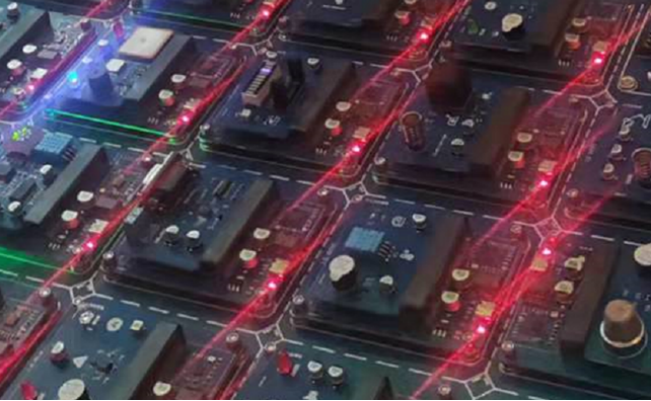
According to Reuters, the U.S. Treasury Department announced new sanctions against Russia, designating 21 entities and 13 individuals as sanctions, including Russia’s largest microelectronics maker Mikron.
According to this executive order, the assets of the above-mentioned objects in the United States will be frozen, and U.S. institutions will be prohibited from doing business with them.
Mikron JSC is Russia's largest microelectronics manufacturer and exports more than 50% of Russia's microelectronics products. The company also produces integrated circuits, electronic components and is Russia's largest chip maker. (Proofreading/Lechuan)
SMIC made revenue of 35.6 billion yuans in 2021, up by 29.7% YOY. Profile was up 147.7% to 10.7 billion yuans. It was the best year in the company's history.
"62.5% of the operation income were from the 90nm process or below, including 29.2% from the 55/65nm process, 15.0% from the 40/45nm process and 15.1% from FinFET/28nm process."
However, the company is having troubles in employee retention. Loss of R&D positions is concerning in particular.
In the last three years, the number of R&D positions in SMIC had been dropping. It was 2530, 2335 and 1758, respectively. Percentage wise, R&D positions vs. total head count was 16.0%, 13.5% and 9.9%, respectively.
In related stats, R&D expenditure vs. revenue was also dropping. It was 21.5%, 17.0% and 11.6% in the last three years, respectively.
In the annual report, SMIC explained that the big loss of R&D positions in 2021 was due to some R&D staff being relocated to help process operations during capacity crunch and the sellout of the subsidiary SJSemiconductor Corporation.
According to SMIC's own published data, from 2018 to 2020 (the most recent update), the company had turnover rate of 22.0%, 17.5% and 17.0%, respectively. In comparison, TSMC had 4.5%, 4.9% and 5.3% in the same period. UMC had 15.4%, 12.1% and 10.3%.
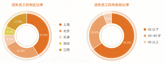
In 2020, more than 40% of those who left the company were working in Shanghai. 65% of those who quit in that year were 30 years old or younger.
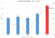

2021年财报披露,中芯国际实现营收356.31亿元,同比增长29.7%;实现净利润107.33亿元,同比增长147.7%;实现扣非净利润53.25亿元,同比增长213.8%。这是中芯国际历史上最好的业绩,也是该公司净利润历史上首次突破百亿元大关。
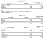
"62.5% of the operation income were from the 90nm process or below, including 29.2% from the 55/65nm process, 15.0% from the 40/45nm process and 15.1% from FinFET/28nm process."
在技术节点方面,来自90纳米及以下制程的晶圆代工业务营收的比例为62.5%。其中,55/65纳米技术的收入贡献比例为29.2%,40/45纳米技术的收入贡献比例为15.0%,FinFET/28纳米的收入贡献比例为15.1%。
However, the company is having troubles in employee retention. Loss of R&D positions is concerning in particular.
In the last three years, the number of R&D positions in SMIC had been dropping. It was 2530, 2335 and 1758, respectively. Percentage wise, R&D positions vs. total head count was 16.0%, 13.5% and 9.9%, respectively.
In related stats, R&D expenditure vs. revenue was also dropping. It was 21.5%, 17.0% and 11.6% in the last three years, respectively.
In the annual report, SMIC explained that the big loss of R&D positions in 2021 was due to some R&D staff being relocated to help process operations during capacity crunch and the sellout of the subsidiary SJSemiconductor Corporation.
According to SMIC's own published data, from 2018 to 2020 (the most recent update), the company had turnover rate of 22.0%, 17.5% and 17.0%, respectively. In comparison, TSMC had 4.5%, 4.9% and 5.3% in the same period. UMC had 15.4%, 12.1% and 10.3%.
In 2020, more than 40% of those who left the company were working in Shanghai. 65% of those who quit in that year were 30 years old or younger.
观察者网查询财报发现,最近三个自然年度末,中芯国际的研发人员数量分别为2530人、2335人和1758人,占总人数的比例分比为16.0%、13.5%和9.9%。与此相关,中芯国际近三年研发投入占营收的比例分别为21.5%、17.0%和11.6%。
中芯国际在2021年财报中提到,本期研发人员数量较上期减少,主要因2021年上半年部分研究相关人员转入生产运营岗位,以及出售子公司SJSemiconductor Corporation影响所致。
观察者网查阅了中芯国际的《企业社会责任报告》,但最新版只更新到2020年。2018年-2020年的数据显示,中芯国际的整体员工流失率分别为22.0%、17.5%和17.0%。作为对比,全球行业龙头台积电这一时期的员工离职率分别为4.5%、4.9%和5.3%;岛内企业联电同期的员工离职率分别为15.4%、12.1%和10.3%,均明显低于中芯国际。
据2020年《企业社会责任报告》披露,上海是中芯国际2020年流失员工最多的地区,占比超过40%;性别上,男性在中芯国际流失员工中占比超过60%;从年龄段看,流失率最高的是30岁以下员工,2020年占比高达65.0%。


Do not be surprised if they join, especially since they now have a Right Wing President. This fellow is probably the most anti-China or at least nationalistic South Korean President since kingdom come... It was understandable as to why Park Chung He was that way towards China... Why Yoon is that way, I wonder why...look like there is ongoing chip alliance discussion between US/taiwan/japan/SK. seem like SK is not onboard yet
Mikron has been sanctioned at least since 2014. They are also part of RTI Systems group who make military radars and are also sanctioned. Remains to seen what the exact change in practical terms is this time.According to Reuters, the U.S. Treasury Department announced new sanctions against Russia, designating 21 entities and 13 individuals as sanctions, including Russia’s largest microelectronics maker Mikron.
According to this executive order, the assets of the above-mentioned objects in the United States will be frozen, and U.S. institutions will be prohibited from doing business with them.
Mikron JSC is Russia's largest microelectronics manufacturer and exports more than 50% of Russia's microelectronics products. The company also produces integrated circuits, electronic components and is Russia's largest chip maker. (Proofreading/Lechuan)
It is time for every major or medium sized power that is industrialized and that has at least moderate levels of modern technological capability comprehensively embark on advanced technological development of any technology worth developing and accordingly create economic systems that enable them to procure materials and also compensate the labour necessary for these things that is thoroughly independent on the Western and any US-backed or dominated financial system.Mikron has been sanctioned at least since 2014. They are also part of RTI Systems group who make military radars and are also sanctioned. Remains to seen what the exact change in practical terms is this time.
Wake up call already happened under Trump.I hope this is a wake up call for Chinese semi industry. But they were already working on their own independence and have been for years.
Huawei explores IC product breakthroughs through advanced packaging and optimizing system architecture
Huawei’s rotating chairman Guo Ping explained Huawei’s IC strategy in the face of the blockade by the U.S. sanctions, saying it is expecting to make breakthroughs in advanced packaging for boosting its chip products at Huawei’s 2021 annual performance conference held on March 28th.

He also revealed that Huawei’s IC company HiSilicon has been upgraded from a second-level business unit to a first-level one alongside Huawei’s Cloud computing and Smart Car Solution, indicating more focus on IC development.
Guo said that with interconnection and stacking of different functional dies, advanced packaging could achieve excellent performance in high-performance semiconductor chips with possible applications in data centers and communication base stations, opening a new generation of IC.
Huawei’s emphasis on system architecture means that advanced packaging will be a critical investment direction for Huawei in manufacturing.
For its breakthroughs through advanced packaging, Huawei reportedly has set up partnerships with Quliang Electronics (渠梁电子), a chip packaging and testing supplier based in Fujian Province, and display giant BOE in panel-level chip packaging technology.
Huawei would use the multi-core structure to support chip architecture reconstruction. “It will revive the life of chips, allowing less-advanced processes to be competitive in future products,” Guo said.
Huawei has made progress in some of its theoretical and architectural breakthroughs. Its Noah’s Ark Lab has come up with the innovative algorithm in the open-sourced AdderNet, reducing AI computing power consumption by 88% and circuit area by 76%. It introduced gallium nitride materials to the power amplifier chip, which consumes the most significant amount of energy of the radio frequency part in its base station equipment, improving amplification efficiency and reducing energy consumption by 20%.
If Huawei can develop the system-level packaging of mature-processed bare chips to achieve outstanding performance for mid-to-low-end shelf products, it can gain a different development window with a market potential worth looking forward to and open a new generation.
The advanced packaging process that integrates the front and rear sections will accumulate Huawei’s proprietary knowledge and workforce reserves in the field of semiconductor manufacturing and lay the foundation for possible future breakthroughs in advanced manufacturing processes.
Huawei’s rotating chairman Guo Ping explained Huawei’s IC strategy in the face of the blockade by the U.S. sanctions, saying it is expecting to make breakthroughs in advanced packaging for boosting its chip products at Huawei’s 2021 annual performance conference held on March 28th.

He also revealed that Huawei’s IC company HiSilicon has been upgraded from a second-level business unit to a first-level one alongside Huawei’s Cloud computing and Smart Car Solution, indicating more focus on IC development.
Guo said that with interconnection and stacking of different functional dies, advanced packaging could achieve excellent performance in high-performance semiconductor chips with possible applications in data centers and communication base stations, opening a new generation of IC.
Huawei’s emphasis on system architecture means that advanced packaging will be a critical investment direction for Huawei in manufacturing.
For its breakthroughs through advanced packaging, Huawei reportedly has set up partnerships with Quliang Electronics (渠梁电子), a chip packaging and testing supplier based in Fujian Province, and display giant BOE in panel-level chip packaging technology.
Huawei would use the multi-core structure to support chip architecture reconstruction. “It will revive the life of chips, allowing less-advanced processes to be competitive in future products,” Guo said.
Huawei has made progress in some of its theoretical and architectural breakthroughs. Its Noah’s Ark Lab has come up with the innovative algorithm in the open-sourced AdderNet, reducing AI computing power consumption by 88% and circuit area by 76%. It introduced gallium nitride materials to the power amplifier chip, which consumes the most significant amount of energy of the radio frequency part in its base station equipment, improving amplification efficiency and reducing energy consumption by 20%.
If Huawei can develop the system-level packaging of mature-processed bare chips to achieve outstanding performance for mid-to-low-end shelf products, it can gain a different development window with a market potential worth looking forward to and open a new generation.
The advanced packaging process that integrates the front and rear sections will accumulate Huawei’s proprietary knowledge and workforce reserves in the field of semiconductor manufacturing and lay the foundation for possible future breakthroughs in advanced manufacturing processes.
- Status
- Not open for further replies.
