Chinese semiconductor industry

Status
Not open for further replies.

ansy1968

Brigadier
Registered Member
We can judge for ourselves, thanks. Let me just remind you that experts know experts, and can always find out who is bullshit and who isn't eventually.
@FairAndUnbiased bro Respect is earned not given, we're open for constructive criticism as most of us are amateurs and want to learn especially the opaqueness of gathering info regarding China IC. And here we're fortunate to have actual esteem members who knew what is happening inside and one of them is @Oldschool and let's hear his opinion.

Oldschool

Junior Member​

Registered Member
12 minutes agoNew
Hi,
I find hvpc statement about disabled SMIC already purchased ASML scanners if it followed US new sanctions is far fetched. It doesnt make sense.

I had a private conversation with him and find no evidences to support it.

First of all, I don't believe there's a technical way to disable scanner remotely. Even if it can be done it's a clear business violation. It's hacker attempt. People already paid for that scanner and it's illegal to hack someone's property. It doesn't make business sense. Companies can sue ASML if it does in China. Chinese government can freeze it's assets and put it out of business.

Businesses are transparent even if it comes to sanctions. If it does follow US new sanction it will tell SMIC upfront it cannot sell them anymore new machines and cannot provide them additional services. For existing already purchased scanners it's all up to SMIC itself to make it work.

Hacking to make SMIC existing paid scanner to nonworking is illegal nor doable.
 

hvpc

Junior Member
Registered Member
28nm. Much of the Chinese military chip production appears to be 40nm and higher. Always remember that the smaller the nm is, the more susceptible the chip is to EM interference, EMP, cosmic rays in the higher atmosphere, and so on, so there is a limit to how far any military will accept smaller and smaller nm. This is why going to another chip making technology like graphene or going to 3D stacking, might be a more attractive idea.

Remember this picture? Note that "20" on the third item should stand for J-20, while the others are for J-16 and J-10B. It also describes the modules used for the "-20" radar uses 3D MCM. The infographic describes three generations of AESA radars, starting with the J-10B at Gen 1.5. The four digits represent the number of elements so the J-10B is 12XX, the J-16 at 1760, and the J-20 at 1856.


View attachment 85418
Question. What do they use to produce 28nm chips? not aware they have immersion system…perhaps they have ebeam litho system? Thanks.
 

tokenanalyst

Brigadier
Registered Member
28nm. Much of the Chinese military chip production appears to be 40nm and higher. Always remember that the smaller the nm is, the more susceptible the chip is to EM interference, EMP, cosmic rays in the higher atmosphere, and so on, so there is a limit to how far any military will accept smaller and smaller nm. This is why going to another chip making technology like graphene or going to 3D stacking, might be a more attractive idea.

Remember this picture? Note that "20" on the third item should stand for J-20, while the others are for J-16 and J-10B. It also describes the modules used for the "-20" radar uses 3D MCM. The infographic describes three generations of AESA radars, starting with the J-10B at Gen 1.5. The four digits represent the number of elements so the J-10B is 12XX, the J-16 at 1760, and the J-20 at 1856.


View attachment 85418
Maybe they manage to produce those chips in low volume, They have been researching lithography for quite some time.

Please, Log in or Register to view URLs content!

Development of 157 nm Lithography​


TONG Zhi-yi GE Mai-chong(The 45th Research Institute of CETC, Beijing East Yanjiao 101601,China )

This paper presents the progress of 157 nm F2 excimer laser lithography as one of Next Generation Lithography (NGL) and the development status of several companies'157 nm exposure tools. Describing various restraint factors in 157 nm lithography, such as the intrinsic birefringence of CaF2material, exhaust purging of vacuum environment and contamination control, pellicles selection, catadioptric optics selectionand design, development of new type resists have been basically solved with the lapse of time. Finally discussesthe possibility of 157 nm lithography to be selected by 45 nm and below node devices pattern exposure, and the potential of 157 nm immersion lithography to be accessed to 32 nm node devices pattern exposure.

But military chips usually don't need the smallest node, they are usually specialty chips were reliability is better than the shiniest node, pretty much like the auto industry.
 

hvpc

Junior Member
Registered Member
Question. What do they use to produce 28nm chips? not aware they have immersion system…perhaps they have ebeam litho system? Thanks.
@FairAndUnbiased bro Respect is earned not given, we're open for constructive criticism as most of us are amateurs and want to learn especially the opaqueness of gathering info regarding China IC. And here we're fortunate to have actual esteem members who knew what is happening inside and one of them is @Oldschool and let's hear his opinion.

Oldschool

Junior Member​

Registered Member
12 minutes agoNew
Hi,
I find hvpc statement about disabled SMIC already purchased ASML scanners if it followed US new sanctions is far fetched. It doesnt make sense.

I had a private conversation with him and find no evidences to support it.

First of all, I don't believe there's a technical way to disable scanner remotely. Even if it can be done it's a clear business violation. It's hacker attempt. People already paid for that scanner and it's illegal to hack someone's property. It doesn't make business sense. Companies can sue ASML if it does in China. Chinese government can freeze it's assets and put it out of business.

Businesses are transparent even if it comes to sanctions. If it does follow US new sanction it will tell SMIC upfront it cannot sell them anymore new machines and cannot provide them additional services. For existing already purchased scanners it's all up to SMIC itself to make it work.

Hacking to make SMIC existing paid scanner to nonworking is illegal nor doable.
?? I never said a supplier could disable the tool remotely.

I pointed that out to @Oldschool I’m our private conversation.

I only said most advanced tools could be accessed remotely for serving or diagnosis.
 

Schmoe

New Member
Registered Member
"Hacking to make SMIC existing paid scanner to nonworking is illegal nor doable." Couldn't, or wouldn't, the embedded software packages built into scanners require an updated code after a specified period of time, or the system locks? Microsoft has figured that out. There are also concerns that Russia might have serious problems due to that issue, although hopefully Russian coders can replace most software.
 

tokenanalyst

Brigadier
Registered Member

A new generation of scene verification tools - GalaxPSS​


16475782173384.gif


As early as 5 years ago, it was predicted that PSS (Portable Stimulus Standard) would become one of the mainstream verification technologies like UVM. Today, in the face of increasingly complex system-level chip verification, in addition to the challenges brought about by the increase in integration scale, a series of new topics, including architecture exploration, software and hardware collaboration, and cross-platform reuse of test cases, are placed in front of chip verification engineers. PSS, which is highly expected by many industry experts, has become a powerful tool to deal with new challenges due to its advantages such as automatic generation of verification scenarios and homologous and portable incentives.

GalaxPSS makes chip verification more time-saving and labor-saving

PSS sounded the prelude to innovation, and EDA manufacturers saw the new technical path. A series of EDA products applying new standards appeared on the drum beat in the preview. In November 2021, Xinhuazhang released a new generation of scenario verification tool GalaxPSS based on the Accellera PSS standard and advanced verification methodology.

Please, Log in or Register to view URLs content!
 

tokenanalyst

Brigadier
Registered Member
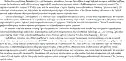
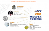
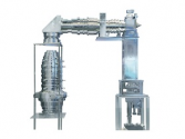
Looks like Beijing E-Town the investment group that acquired the Rapid thermal processing company Mattson created the subsystem provider Beijing Guowang Optical Technology, that are the ones who are going to mass produce the optics for different lithography systems in China and they themselves acquired CNEPO the company who developed the Epolith A075 Exposure Optical System for the SMEE Arf Machines.

1647583091957.png

1647583150012.png

1647583276368.png
1647583398842.png
 
Status
Not open for further replies.
Top