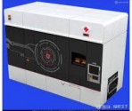
Which foreign equipment supplier would this advancement replace?745 x 1100 mm exposure region with 0.5 um resolution is incredible and world class. Let me explain.
Linear resolution per exposure area is a measure of the alignment precision required of an instrument. Typically as dimensions get larger, tolerances also get larger since tolerances are usually described as % deviations. So how tight are the tolerances here?
745x1100 mm exposure area with 0.5 um resolution is linear resolution per exposure area of 1.22x10E-6 um/mm2.
For comparison, ASML TwinScan EUV has 13 nm (0.013 um) resolution exposed for 26x33 mm.
That is linear resolution per exposure area of 1.43x10E-5 um/mm2.
The tolerances required for precision UV exposure of such a huge area is tighter than that of even EUV.
You are using an out of date browser. It may not display this or other websites correctly.
You should upgrade or use an alternative browser.
You should upgrade or use an alternative browser.
Chinese semiconductor industry
- Thread starter Hendrik_2000
- Start date
- Status
- Not open for further replies.
Which foreign equipment supplier would this advancement replace?
comparable in terms of substrate size, resolution, overlay accuracy and exposure time.
overall I'd rate SMEE as being close to Japanese lithography manufacturers like Canon and Nikon. However with an ArF scanner, SMEE does have something that Canon doesn't have.
@FairAndUnbiased bro can you kindly explain what it is? I know in DUVL Nikon have something special with a Litho comparable with NXT 2050i in 2023.
comparable in terms of substrate size, resolution, overlay accuracy and exposure time.
overall I'd rate SMEE as being close to Japanese lithography manufacturers like Canon and Nikon. However with an ArF scanner, SMEE does have something that Canon doesn't have.
SMEE has a ArF scanner, Canon only has KrF.@FairAndUnbiased bro can you kindly explain what it is? I know in DUVL Nikon have something special with a Litho comparable with NXT 2050i in 2023.
Yes, from being a company the just offered 1 product:
comparable in terms of substrate size, resolution, overlay accuracy and exposure time.
overall I'd rate SMEE as being close to Japanese lithography manufacturers like Canon and Nikon. However with an ArF scanner, SMEE does have something that Canon doesn't have.
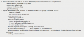
To a company that offer a broader range of products.
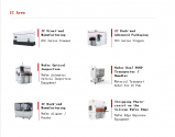
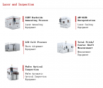
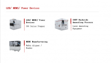
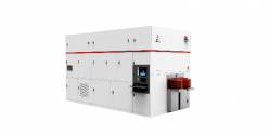
Also i don't think Canon offer products for IGBT, robots and measurement equipment.
Attachments
I believe that shanghai microelectronics equipment is the underdog of the semiconductor industry, and I don't think they deserve the hate they get because they don't offer YET what ASmL produces, I think they have worked hard and developed good equipment.In 2017, He Rongming, the then general manager of Shanghai Microelectronics, had gray hair. In an interview with Jiefang Daily, he said calmly, "I really have nothing to write about, and I can't tell the wonderful stories you want to hear. It has been done for ten years.” "Except for business trips, I go out at 7 am every day, go home at 10 pm every day, I guarantee no rest on Saturdays, and no guarantees for rest on Sundays. This is the whole of my life for more than ten years."
Their recently announced SSB520 lithography machine i think offer higher resolution and wider area for advance packaging than most of what is out there in the market including from Veeco, Rudolph and Canon.
@WTAN Sir a question, how many units of DUVL will SMEE produce this year 6 sets? 1 unit per 2 months? discounting the fact that a delay of 1 month due to Chinese new year?
And also is this the Shanghai FAB
Yes this is the Shanghai FAB which is in collaboration with ICRD.@WTAN Sir a question, how many units of DUVL will SMEE produce this year 6 sets? 1 unit per 2 months? discounting the fact that a delay of 1 month due to Chinese new year?
And also is this the Shanghai FAB with collaboration with ICRD?
The Shanghai FAB is already up and running and already produces 45nm ICs since late 2021.
The FAB has been extended and is now ready to produce 28nm ICs.
The 14nm Production Line will also eventually be at this FAB.
The alleged Joint Venture FAB with SMIC in Shenzhen that is getting Biden's Underwear in a twist is probably just a rumour.
Huawei has all the technical capabilities to run its own FABs with ICRDs help.
No need to involve SMIC. Huawei already is a shareholder in SMEE.
SMEE is very busy at the moment and is shipping out the 90nm, 65nm and its new Advanced Packaging Lithograph.
The production of its SMEE 28nm DUVL should be ramping up in 2022.
They should be shipping out more than 6 units this year.
But of course production will be detemined by how many units of the 60W Arf Light Sources they can be supplied with.
But Huawei will be their No1 customer for DUVL.
@WTAN thanks Sir as always, much obliged.Yes this is the Shanghai FAB which is in collaboration with ICRD.
The Shanghai FAB is already up and running and already produces 45nm ICs since late 2021.
The FAB has been extended and is now ready to produce 28nm ICs.
The 14nm Production Line will also eventually be at this FAB.
The alleged Joint Venture FAB with SMIC in Shenzhen that is getting Biden's Underwear in a twist is probably just a rumour.
Huawei has all the technical capabilities to run its own FABs with ICRDs help.
No need to involve SMIC. Huawei already is a shareholder in SMEE.
SMEE is very busy at the moment and is shipping out the 90nm, 65nm and its new Advanced Packaging Lithograph.
The production of its SMEE 28nm DUVL should be ramping up in 2022.
They should be shipping out more than 6 units this year.
But of course production will be detemined by how many units of the 60W Arf Light Sources they can be supplied with.
But Huawei will be their No1 customer for DUVL.
Are the 45 nm and 28 nm fully domestic? If yes, then this is huge news.Yes this is the Shanghai FAB which is in collaboration with ICRD.
The Shanghai FAB is already up and running and already produces 45nm ICs since late 2021.
The FAB has been extended and is now ready to produce 28nm ICs.
The 14nm Production Line will also eventually be at this FAB.
The alleged Joint Venture FAB with SMIC in Shenzhen that is getting Biden's Underwear in a twist is probably just a rumour.
Huawei has all the technical capabilities to run its own FABs with ICRDs help.
No need to involve SMIC. Huawei already is a shareholder in SMEE.
SMEE is very busy at the moment and is shipping out the 90nm, 65nm and its new Advanced Packaging Lithograph.
Would it be possible to reach 7 nm on this machine using multi-patterning or the limit is around 14 nm?The production of its SMEE 28nm DUVL should be ramping up in 2022.
They should be shipping out more than 6 units this year.
But of course production will be detemined by how many units of the 60W Arf Light Sources they can be supplied with.
But Huawei will be their No1 customer for DUVL.
- Status
- Not open for further replies.

