Last edited:
You are using an out of date browser. It may not display this or other websites correctly.
You should upgrade or use an alternative browser.
You should upgrade or use an alternative browser.
Chinese semiconductor thread II
- Thread starter vincent
- Start date
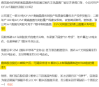
Two Dinglong Technology produced high end photoresists have passed verification by major domestic wafer foundries and secured orders.
Dinglong Technology has achieved significant progress in domestically produced high-end wafer photoresists, with two KrF and ArF photoresists passing verification by major Chinese semiconductor foundries and securing orders. This marks a critical step toward reducing reliance on imported materials amid global supply chain decoupling.
With over 30 high-end photoresist products covering KrF and immersion ArF processes, Dinglong has established an independent R&D and manufacturing system from raw materials to finished goods, underpinned by a "self-developed R&D + vertical integration" strategy. Its Qianjiang Phase I factory currently supports annual production of 30 tons, with plans to scale up to 300 tons via a 910 million yuan convertible bond issuance (480 million yuan allocated for industrialization).
View attachment 166730
Beyond photoresists, Dinglong is a leader in semiconductor CMP materials the only domestic company fully mastering the core technology and process of CMP polishing pads, with strong growth in polishing slurries and cleaning fluids. In H1 2025, its CMP segment revenues rose by over 59% year-on-year, including first-time orders for copper polishing slurry.
This breakthrough strengthens China’s semiconductor supply chain security, demonstrating Dinglong's capability to provide stable, high-performance domestic alternatives in key bottleneck materials.
This is good news. I think there are now multiple Chinese photoresist suppliers for KrF and ArF/ArFi process. It is more a matter of just how much production they have that's still the problem. 30t is really little. And even 300t sounds like not very much here. So, we need a whole bunch of domestic suppliers.
I don't know why iPhone dominates the flagship segment so much in China. Most celebrities (espescially 99% of the female) always use an iPhone.So no, Kirin chip production is not the main issue for Huawei. The main issue is that China's high end phone market is only so large and iPhone continue to dominate the market share and Xiaomi 15/17 is also in there now, so it is not possible for Huawei to actually sell 20 million of flagship Mate/Pura phones per year right now.
This is a bit misleading. They make it sound like existing tariffs on Chinese chips have been removed, which is not the case.
This is a totally new tariff they just introduced (currently set at 0% which is to be increased in 2027). It's a tariff specifically for semiconductors that applies on top of the existing tariffs like "fentanyl tariff". They did not remove the existing tariffs.
US labels Chinese chips an economic threat, but delays tariff impact until 2027
In a formal notice of action filed with the Federal Register, the agency said the US is implementing a tariff action on a wide range of Chinese semiconductors, with an initial rate of 0 per cent. The rate is set to rise in 18 months, on June 23, 2027, to a higher level that will be announced 30 days before the deadline.
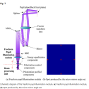
Fast micromirror selection and angle setting algorithm for freeform pupil in the illumination system for immersion lithography machines.
Abstract
As lithography resolution improves, the performance requirements for illumination pupils in immersion lithography machines have become increasingly stringent, particularly regarding energy balance and polarization properties. These characteristics are primarily achieved by adjusting the angular distribution of the micromirror array (MMA). For technology nodes below 40 nm, the impact of light polarization on imaging must be considered. This paper proposes a micro-mirror selection and angle setting algorithm to maintain key characteristics of the freeform pupil, ensuring energy balance in both unpolarized and polarized states. Energy balance in the unpolarized state is influenced by the eccentricity of light, while energy balance in the polarized state depends on both the eccentricity and polarization properties of light. To validate the accuracy of the algorithm, simulations were conducted using freeform pupil illumination optical models for both unpolarized and polarized states. The results demonstrated a significant improvement in energy balance, with a reduction to 0.08% in both states. For engineering applications, the computational speed of the algorithm was enhanced, reducing the calculation time from 600 to 0.1 s.

Moire-Based Overlay Metrology Enhanced by Deep Learning.
Abstract:
Overlay (OVL) is one of the three critical metrics in Photolithography. As technology advances and critical sizes shrink, sub-nanoscale overlay metrology has become a major challenge. Diffraction superposition (DBO) technology is widely used for overlay metrology, with increasing attention on the circular moiré-based DBO method due to the symmetry, isotropy, and non-periodic nature of circular gratings. However, traditional analytical methods for circular moiré fringes suffer from low precision, limited to the tens of nanometers range. In this paper, we propose a hybrid deep learning architecture that combines wavelet convolution, octave convolution, and the Swin Transformer block for enhanced overlay accuracy. Our approach achieves sub-nanoscale overlay by using the overlay marks of circular grating marks in both x and y directions. Furthermore, this strategy demonstrates exceptional robustness to noise induced by the etching and chemical mechanical polishing processes.
Significant breakthrough in SiC technology! Hanteng Technology launches world's first 12-inch silicon carbide epitaxial wafer.
Hanteng Technology has launched the world’s first 12-inch silicon carbide (SiC) epitaxial wafer, marking a major breakthrough in SiC semiconductor technology. This 300mm wafer significantly boosts production efficiency offering 4.4 times more chips than 6-inch wafers and 2.3 times more than 8-inch wafers leading to lower unit costs and greater scalability for power devices.
SiC semiconductors offer superior performance in high-frequency, high-voltage, and high-temperature applications, enabling energy-efficient, compact systems used in new energy vehicles, solar power, AI systems, rail transit, smart grids, and aerospace. With global demand expected to surge projected at over 100 million 12-inch Si wafers by 2025—the industry is rapidly entering the 12-inch era, where technological leaders will dominate.
Hanteng Technology is a pioneer in China’s SiC wafer development: it was the first to achieve commercial production of 3–6-inch SiC wafers and became the first in Greater China to break through 8-inch technology. In 2024, it became the only global company to mass-sell 8-inch SiC epitaxial wafers. It was named a National Manufacturing Single Champion and recognized as a leading specialized and innovative small giant enterprise.
The new 12-inch wafer is built on fully domesticated supply chains: epitaxy equipment from Qiushi Semiconductor (Jingsheng ME) and substrates from Zhejiang Jingrui (SuperSiC), both subsidiaries of Jingsheng Mechanical & Electrical. The wafer meets high reliability standards with:
- Epitaxial layer non-uniformity ≤3%
- Doping concentration non-uniformity ≤8%
- Yield of 2mm×2mm chips >96%
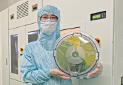
Hanteng is also the world’s largest supplier of SiC epitaxial wafers (2023), with a global market share exceeding 31% in 2024, and has led the development of the first international SEMI standard for 4H-SiC homo-epitaxy (SEMI M092-0423).
The company is now preparing for mass production, positioning itself as a key player in the global transition to large-scale, low-cost SiC-based power electronics.
Sukos Semiconductor's 4.5G glass-based TGV advanced coating equipment (large board size 730mm*920mm) has been successfully shipped.
On December 13, 2025, Sukos (Jiangsu) Semiconductor Equipment Technology Co., Ltd. achieved a significant milestone in the field of advanced packaging equipment—its 4.5G glass-based TGV advanced coating equipment completed production debugging and was officially shipped to leading domestic advanced packaging companies.
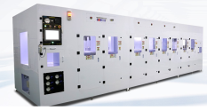
This shipment is a 730*920mm large-panel TGV electroplating equipment adapted to 4.5-generation (G4.5) lines. This signifies the company's technological iteration and continuous mass production capabilities.
Compared to traditional small-sized (e.g., 510*515mm) 730*920mm "large-panel" equipment, it significantly increases the number of chips produced per batch and substantially reduces unit costs, representing a crucial step towards large-scale commercial applications.
Huahai Qingke Signs Agreement with Jinqiao! Settles in Shanghai
According to the official WeChat account of Jinqiao Group, Huahai Qingke (Shanghai) Semiconductor Co., Ltd. (hereinafter referred to as "Huahai Qingke"), a leading domestic integrated circuit equipment enterprise, recently signed an agreement to settle in Jinqiao Equipment Town Innovation Park. Leveraging the industrial ecosystem of Jinqiao Equipment Town, it will establish its Shanghai headquarters integrating R&D, production, sales, procurement, and service, focusing on high-end integrated circuit equipment for advanced processes and advanced packaging.
It is reported that with its establishment in Jinqiao Equipment Town, Huahai Qingke's main business and products in Shanghai will focus on ion implantation equipment, chemical mechanical polishing equipment, and high-precision grinding equipment for advanced processes and advanced packaging. In this initial phase, a Shanghai R&D and production center will be established. This center will closely follow the evolving process nodes of key customers in Shanghai and the Yangtze River Delta region, moving towards smaller process nodes and richer emerging application scenarios such as 3D IC advanced packaging. It will continuously develop and improve product performance and key technical indicators, and rapidly expand production capacity to meet the needs of key customers in Shanghai and the Yangtze River Delta region who have established advanced process and advanced packaging production lines. Simultaneously, it will build a customer technical service center and inventory management center for the Yangtze River Delta region to enhance customer service capabilities and response speed, improve the operational efficiency of maintenance and PM technical service businesses, and provide first-class technical services to customers in Shanghai and the Yangtze River Delta region.
I will add more....
Two Dinglong Technology produced high end photoresists have passed verification by major domestic wafer foundries and secured orders.
Dinglong Technology has achieved significant progress in domestically produced high-end wafer photoresists, with two KrF and ArF photoresists passing verification by major Chinese semiconductor foundries and securing orders. This marks a critical step toward reducing reliance on imported materials amid global supply chain decoupling.
With over 30 high-end photoresist products covering KrF and immersion ArF processes, Dinglong has established an independent R&D and manufacturing system from raw materials to finished goods, underpinned by a "self-developed R&D + vertical integration" strategy. Its Qianjiang Phase I factory currently supports annual production of 30 tons, with plans to scale up to 300 tons via a 910 million yuan convertible bond issuance (480 million yuan allocated for industrialization).
View attachment 166730
Beyond photoresists, Dinglong is a leader in semiconductor CMP materials the only domestic company fully mastering the core technology and process of CMP polishing pads, with strong growth in polishing slurries and cleaning fluids. In H1 2025, its CMP segment revenues rose by over 59% year-on-year, including first-time orders for copper polishing slurry.
This breakthrough strengthens China’s semiconductor supply chain security, demonstrating Dinglong's capability to provide stable, high-performance domestic alternatives in key bottleneck materials.
