We describe a reduced instruction set computing architecture (RISC-V) microprocessor capable of executing standard 32-bit instructions on 5,900 MoS2 transistors and a complete standard cell library based on 2D semiconductor technology.

You are using an out of date browser. It may not display this or other websites correctly.
You should upgrade or use an alternative browser.
You should upgrade or use an alternative browser.
Chinese semiconductor thread II
- Thread starter vincent
- Start date
Interesting Achievement. ALD has been the cornerstone of transistors miniaturization apart from lithography, this is many times more thinner than ALD films.
According to Fudan University, the joint team of Zhou Peng and Bao Wenzhong from the National Key Laboratory of Integrated Chips and Systems of Fudan University has successfully developed the world's first 32-bit RISC-V architecture microprocessor based on two-dimensional semiconductor materials - "WUJI".
This achievement has broken through the bottleneck of two-dimensional semiconductor electronics engineering and achieved the integration of 5,900 transistors for the first time. It is a domestic technology completed by the Fudan team with independent intellectual property rights, which enables my country to take the first-mover advantage in the development of new generation chip materials and provides strong support for promoting electronic and computing technology into a new era. The relevant results were published in the journal Nature on the evening of April 2, Beijing time, under the title "A RISC-V 32-Bit Microprocessor Based on Two-dimensional Semiconductors".
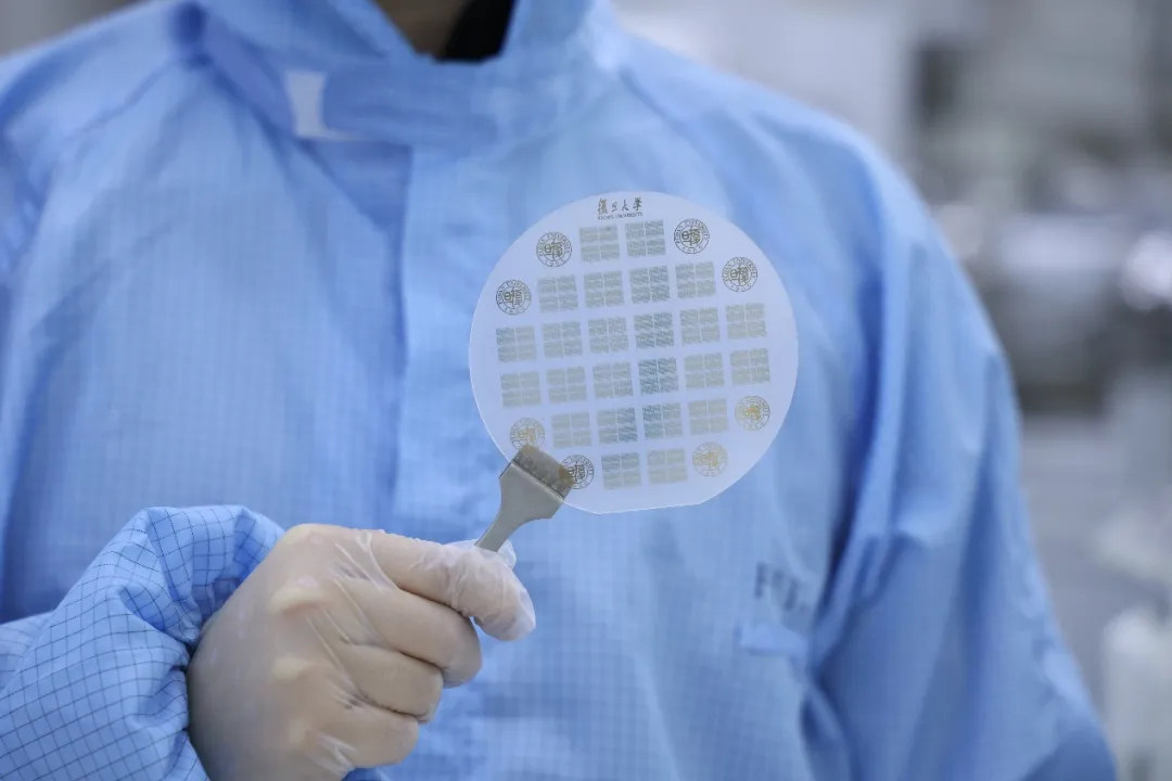
According to Fudan University, over the past decade, the international academic and industrial communities have mastered the wafer-level two-dimensional material growth technology and successfully manufactured high-performance basic devices with hundreds of atoms in length and several atoms in thickness. However, before the Fudan team made a new breakthrough, the world's highest two-dimensional semiconductor digital circuit integration was only 115 transistors, which was achieved by the team of the Vienna University of Technology in Austria in 2017 .
The core difficulty is that assembling these atomic-level precision components into a complete integrated circuit system is still subject to the coordinated yield control of process accuracy and scale uniformity. After five years of research, the Fudan team pushed the chip from array level or single tube level to system level integration, and the 32-bit RISC-V architecture microprocessor "WUJI" based on two-dimensional semiconductor materials (molybdenum disulfide MoS2) was successfully launched.
The chip integrates 5,900 transistors through independent innovative special integration technology and the open source simplified instruction set computing architecture (RISC-V), setting the world's largest-scale verification record for two-dimensional logic chips .
According to Zhou Peng, a professor at the School of Microelectronics at Fudan University, two-dimensional materials are not like silicon wafers that can be grown into high-quality large-size single crystals through the Czochralski method, but need to be grown through chemical vapor deposition (CVD), which leads to defects and inhomogeneities in the material itself. The inverter yield in this study is as high as 99.77%, with excellent performance such as single-stage high gain and ultra-low leakage in the off state, which is an engineering breakthrough.
According to Ao Mingrui, the co-first author of the paper and a direct doctoral student at the School of Microelectronics, the team manufactured 900 inverter arrays, each containing 30×30 inverters. After rigorous testing, it was found that the logic functions of 898 of the inverters were intact, and the flip voltage and dispute value were very ideal, leading similar research .
As an open source simplified instruction set computing architecture, RISC-V has gradually become the mainstream choice in the current chip research and development field. The chip developed this time uses the RISC-V architecture as the design basis. Han Jun, a researcher at the School of Microelectronics, is responsible for the design of the RISC-V architecture in this work. He introduced that choosing this architecture means connecting to global technical standards without relying on closed architectures. In the future, it can independently build a user ecosystem without being restricted by the architecture and IP patents of foreign manufacturers.
In the two-dimensional semiconductor integration process developed by the team, about 70% of the processes can directly use the mature technology of existing silicon-based production lines, and the core two-dimensional characteristic process has also built an independent technology system including more than 20 process invention patents, combined with special process equipment, paving the way for industrialization. In the next step, the team will further improve the chip integration, find and build a stable process platform, and lay the foundation for the development of specific application products in the future.
Junyuan Electronics Semiconductor Electrostatic Chuck Project Signed and Settled in Wuhan Optics Valley
According to China Optics Valley, on April 2, Junyuan Electronics signed a contract with Wuhan East Lake High-tech Zone to build a semiconductor electrostatic chuck project in Optics Valley.
Junyuan Electronics was established in 2020. It has the full-process capabilities of semiconductor electrostatic chucks (ESC) from research and development to mass production. Its products cover the main etching machine applications of 14 nanometers and above, and have been verified by domestic 12-inch wafer fabs. Wang Ji Zeng, general manager of Junyuan Electronics, said that the project settled in Optics Valley will further narrow the distance with Optics Valley integrated circuit companies, reduce logistics costs, and improve product application efficiency. In the future, the company will cooperate with upstream and downstream companies in the local industrial chain to continuously break through semiconductor electrostatic chuck technology and strive to become a global technology-leading supplier of integrated circuit core components.
As one of the core components of wafer production equipment, the electrostatic chuck is a ceramic tray that uses static electricity to absorb and transport wafers. It is like the "invisible hand" of chip manufacturing. It is used in etching machines, photolithography machines, and coating equipment to fix the wafer and ensure that it does not move. Due to the high difficulty in manufacturing ceramic materials and precision electrodes, the production technology of semiconductor electrostatic chucks is one of the important technologies that domestic companies need to overcome in promoting the localization of chip manufacturing.
The signed project is located in the Optics Valley Zhuxin Technology Industrial Park in the Future Science and Technology City. It will build an electrostatic chuck production line to provide electrostatic chuck production and maintenance services for Optics Valley integrated circuit companies nearby
Last edited:
An extreme ultraviolet motor system for photolithography machine

A projection lithography machine alignment sensing system based on grating and lens group integration

Illumination system, photolithography machine, and illumination uniformity compensation method

ZnSe and diamond lens material supplier to Trumpf’s EUV CO2 laser.
Vacuum tube supplier for Trumpf’s CO2 laser RF source and domestic (UEAscend?) EUV CO2 laser
公司开发的多个型号大功率电子管,已顺利通过国产光刻机客户的验证并实现批量供货
Huahai Qingke's patent for "a wafer scrubbing device, a wafer scrubbing system and a polishing device" was published.
Huahai Qingke Co., Ltd.'s patent for "a wafer scrubbing device, a wafer scrubbing system and a polishing device" has been announced. The application publication date is February 28, 2025, and the application publication number is CN119542201A.

The embodiment of the present application provides a wafer scrubbing device, a wafer scrubbing system and a polishing device, wherein the wafer scrubbing device includes: a scrubbing brush and a scrubbing brush control module; the scrubbing brush control module is arranged on the side of the scrubbing brush facing away from the wafer, and includes a telescopic module and a magnetic module arranged in sequence toward the scrubbing brush; the scrubbing brush includes a first rotating shaft and a brush head, the first rotating shaft includes a first end facing the wafer and a second end facing away from the wafer, the first end of the first rotating shaft is connected to the brush head, and the second end is magnetically connected to the magnetic module; the scrubbing brush control module is configured to control the scrubbing pressure between the scrubbing brush and the wafer through the axial telescopic movement of the telescopic module. The present application realizes a flexible magnetic connection between the scrubbing brush and the scrubbing brush control module through the arrangement of the magnetic module and the telescopic module, and can keep the pressure applied by the brush head to the wafer surface constant during the scrubbing process.
The embodiment of the present application provides a wafer scrubbing device, a wafer scrubbing system and a polishing device, wherein the wafer scrubbing device includes: a scrubbing brush and a scrubbing brush control module; the scrubbing brush control module is arranged on the side of the scrubbing brush facing away from the wafer, and includes a telescopic module and a magnetic module arranged in sequence toward the scrubbing brush; the scrubbing brush includes a first rotating shaft and a brush head, the first rotating shaft includes a first end facing the wafer and a second end facing away from the wafer, the first end of the first rotating shaft is connected to the brush head, and the second end is magnetically connected to the magnetic module; the scrubbing brush control module is configured to control the scrubbing pressure between the scrubbing brush and the wafer through the axial telescopic movement of the telescopic module. The present application realizes a flexible magnetic connection between the scrubbing brush and the scrubbing brush control module through the arrangement of the magnetic module and the telescopic module, and can keep the pressure applied by the brush head to the wafer surface constant during the scrubbing process.
Total investment of 1.1 billion yuan! A project to produce 300,000 pieces of indium phosphide single crystal substrates per year was established in Jiangmen
According to the Jiangmen Kaiping Cuishan Lake Management Committee, Guangdong Pingrui Jingxin Semiconductor Co., Ltd. with a total investment of 1.1 billion yuan has recently signed a contract. Liang Yiqin, chairman of Guangdong Pingrui Jingxin Semiconductor Co., Ltd. and relevant leaders from Jiangmen and Kaiping attended the signing ceremony.
It is reported that Guangdong Pingrui Jingxin Semiconductor Co., Ltd. is a private high-tech enterprise integrating R&D, production and marketing. It mainly focuses on the R&D and application of semiconductor materials such as indium phosphide and gallium arsenide. Its semiconductor material products are widely used in key links of data center systems and electronic smart chips. It will provide strong support for Kaiping to strengthen the new generation of electronic information industry and accelerate the construction of a modern industrial system.
The Guangdong Pingrui Jingxin Semiconductor Technology Industrial Park project is invested and controlled by Guangdong Pingrui Jingxin Semiconductor Co., Ltd., which is mainly engaged in the production of indium phosphide single crystal substrates and belongs to the semiconductor materials industry. The total investment of the project is 1.1 billion yuan, the land area is about 100 acres, and it is expected to produce 300,000 indium phosphide single crystal substrates annually, and the annual sales revenue is expected to exceed 600 million yuan.
CETC showcase their semiconductor manufacturing equipment and materials
In the field of semiconductor materials, the company showcased its core product matrix including silicon carbide crystal substrates and epitaxy, silicon epitaxy, and silicon-based gallium nitride epitaxy. The world's first 12-inch high-purity semi-insulating silicon carbide single crystal substrate attracted much attention. The usable area of a single wafer of this product is 2.25 times that of an 8-inch wafer, which will greatly accelerate the application of silicon carbide materials in new scenarios such as AR glasses and heat sink materials.

In the field of integrated circuit equipment, key equipment achievements such as ion implanters, chemical mechanical polishing equipment, vertical furnaces, wet cleaning, thinning and dicing are displayed. Among them, ion implantation equipment has formed a full range of products including medium beam, large beam, high energy, special, and compound semiconductors, with a strong pace of industrial development, ranking first in China. Chemical mechanical polishing equipment has been upgraded and iterated, and vertical furnaces, thinning equipment, and cleaning equipment have moved towards high-end development, achieving new application breakthroughs, and new momentum is constantly accelerating.

In the field of compound semiconductor equipment, a number of new research results such as defect detection equipment and coating equipment were displayed. "For the detection field, we are fully engaged in the research and development of compound semiconductor defect detection equipment, and are committed to forming a series of products to fill the gaps in the industry." Technical experts said that a series of equipment such as 8-inch silicon carbide single crystal growth, epitaxy, oxidation/annealing, etc. have been introduced to leading companies in batches. The market response to silicon carbide coating equipment is very good. The newly developed carbide coating equipment is undergoing process verification, and the product spectrum is gradually expanding.