They already has 20 yr old EDA company "Huada Empyrean" specializing in analog EDA but lately branch into digital semi They have a good EDA up to 28nm. Compare to jet engine I don't think designing EDA is such a big hurdle, Certainly there are problme One of the biggest is the reluctant of semi company to use and, or collaborate with domestic EDA, of course lack of investment or money. But now since the door is shut thye have no other alternative coupled with massive infusion of money they should have no problem in 2 or 3 years
Here is the status of EDA in China
Here is the profile of Empyrean old 2012
by
Paul McLellan on 05-02-2012 at 8:30 pm
Categories:
,
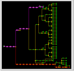
There’s this EDA company. They have over 100 tapeouts. They have a $28M in funding. They have 250 people. And you’ve never heard of them. Or at least I hadn’t.
They are ICScape. They started in 2005 with an investment from Acorn Campus Ventures and delivered their first product, ClockExplorer, in 2007 and their second, TimingExplorer in 2009. They then have gone on to develop a complete openAccess-based place and route system including placement, clock-tree-synthesis, routing, static timing analysis, parasitic extraction and…
In 2008-2010 during the technology downturn they survived purely on product revenue. They turned their attentions to China, which was one area that was still buoyant. Also in China is a 20 year old EDA company called Huada Empyrean Software (HES) who have an openAccess-based analog environment. HES is a subsidiary of China Electronics Corporation, China’s largest electronics conglomerate (and an SOE). HES want to expand outside of China and become a global player, so it was spun out of CEC and merged with ICScape and provided with $28M in funding. They have one engineering organization. HES sells the whole product line in China and Taiwan. ICScape everywhere else (the US, Korea and Japan today, and Europe soon).
They have big plans to become a big global EDA player. I have no idea how good their technology is but they claim that over 100 chips have been taped out, including some at the 28nm technology node, so it should be pretty solid. Customers include Marvell, Huawei, ZTE, NHK and more.
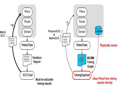
The SoC product line is based around accelerating design closure by reducing the number of iterations by 50%. It consists of four tools:
- TimingExplorer, a physically aware multi-corner, multi-mode timing ECO tool
- ClockExplorer, which can reduce clock insertion delay by up to 50% and clock-tree power by 40%
- Skipper, a high-performance and ultra-large capacity chip finishing solution
- FlashLVL, a high-speed layout comparison tool
The analog product line is now in its 6th generation. It is focused on big-A small-D designs with lots of analog and limited amounts of digital. It contains:
- interconnect-aware layout editing
- high-capacity parallel circuit simulation
- hierarchical parallel physical verification
- mixed-mode, multi-corner parasitic extraction and analysis
Going forward the plan is to bring all the technologies together, which is not such a daunting task as it might be since both product lines are native OA-based. At the same time expand their channel to have complete coverage everywhere.
Here is the problem with Chinese EDA
What holds Chinese EDA back?
Comprehensiveness: Chinese tools are simply not comprehensive enough, especially in digital design. Most of the digital design process is dominated by Synopsys and Cadence. Even if in one or two parts of the design flow Chinese companies have technically competitive products, it is difficult to break into the market as the Big Three have the ability to support customers’ development from spec to production. Chinese companies need to create a total solution to begin competing locally on any level, but even then, it will be difficult due to other factors.
Talent: Most of China’s EDA tool development engineers actually work for the Big Three: of the 1,500+ such engineers in China,
(in Chinese) work for domestic companies. To put things further in perspective, Synopsys on its own globally has over 5,000 such engineers. Would-be EDA entrants also have to compete for talent with more lucrative industries. Application level software development at Alibaba, Tencent, etc. pays much better than a struggling Chinese EDA company.
Market Entry: With 95% of the domestic market, belonging to the Big Three, it is a highly difficult market to enter. Even if a full set of tools could be developed, in the short-term it will be difficult for any fourth company to gain any significant market share. Companies are used to certain design flows and engineers have used tools from the Big Three since university. These difficulties have made the domestic EDA industry a less attractive target for investors and, in turn, limited development.
Integration with Advanced Process Nodes: The link between design and process is a key part of an EDA flow. The Big Three work with the world’s leading wafer plants and foundries to develop a strong understanding of their processes, whereas domestic companies often only have access after a new process is developed and even then, not necessarily complete access. This makes it difficult for domestic companies to design and improve their software to compete with the Big Three.
Piracy: As mentioned above, EDA tool piracy is rife in China. These tools aren’t cheap. Silicon IP can’t be “cracked,” but tools can be. Any domestically focused company looking to save money will save it here. This also means the government may see EDA tool investment as a lower priority, as it can still have access to the tools for military chip design for example, even if bans are in place.
State-backed EDA
The government is beginning to support EDA tool development to some extent, and I expect support to increase over the coming years. Such companies can now claim back 30% of their development costs from the government, capped at RMB 30 million (about $4.3 million).
The government has also helped individual companies. For example, the Guowei Group has been granted
from the central and Shenzhen government for EDA development work. Also, Huada Emperyan has received hundreds of millions in funding over the past couple of years, not just from VCs but also from the state-run “Big Fund.”
While such government help is obviously welcome and is of some assistance it is nothing compared to the Big Three’s internal R & D investments, and if China really wants to become independent in this field much more needs to be done. The recently announced new Chinese government $29 billion semiconductor fund, or “Big Fund Mark Two” as I will call it, may go some way to help, but it remains to be seen how much of this will be invested into EDA. I suspect a small amount compared to how much is invested into memory, foundry capital equipment, and traditional fabless design.
Conclusion
China’s current predicament opens up opportunities for domestic companies. Government investment, coupled with a large domestic market, means they potentially have the environment to grow and improve. China needs to do this in a gradual way though, and not let such companies rely too much on government support. Switching everything to a Chinese equivalent (if one ever exists) could mean slower time to market and worse end products. Adopting a national procurement policy across the board is risky and could discourage innovation. Only once a domestic tool or entire design flow is on a more or less level playing field should they switch, and support should be based on certain milestones to avoid creating SOE-like inefficient operations.
I can see a future where domestic companies compete domestically within China for certain chips, e.g. analog designs or simpler IoT designs. Globally this will be more difficult though, and without access to the most advanced technologies from foreign wafer companies and foundries domestic EDA companies will always be at a disadvantage. China can reduce its dependency but at least for now, has no way of being completely independent in this space.

 , to the point that officials have to come forward to rebuff it.