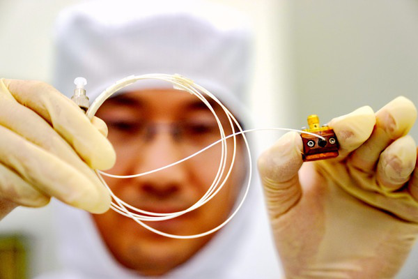
China is making progress of the lithography machine and reach 22nm level it won't belong before they reached 14 nm or even 10nm
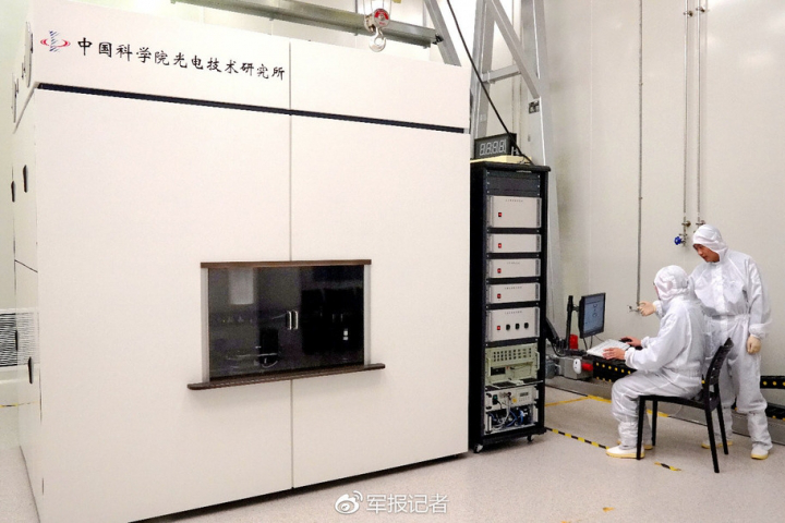
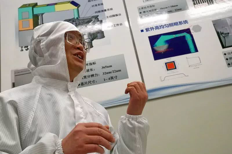
Hu Song said that the lithography machine has a maximum linewidth resolution of 22 nm in a single exposure at a wavelength of 365 nm, which is equivalent to 1/17 wavelength. In principle, the project breaks through the resolution diffraction limit and establishes a new high-resolution, large-area nanolithography equipment research and development route. It has completely independent intellectual property rights
China created the first independent new lithography machine, which can make 10nm chips in the future.
Hu Song, deputy director of the Institute of Optoelectronic Technology of the Chinese Academy of Sciences, revealed that the newly accepted lithography machine has a processing capability between the deep ultraviolet and the extreme ultraviolet, and uses a 365 nm ultraviolet mercury lamp. Ten thousand yuan, and the price of the whole lithography machine is in the range of one million yuan to ten million yuan, "let many users overjoyed"...
On November 29th, Beijing time, the Institute of Optoelectronic Technology of the Chinese Academy of Sciences announced that the National Research and Development Equipment Development Project “Super Resolution Lithography Equipment Development” passed the acceptance test and became the world's first 22nm resolution lithography machine realized by ultraviolet light source.
According to China Science and Technology Daily, Hu Song, deputy director of the Institute of Optoelectronic Technology of the Chinese Academy of Sciences, revealed that the newly accepted lithography machine uses a 365 nm UV mercury lamp, a cost of only tens of thousands of dollars, while lithography The price of the whole machine is in the range of one million yuan to ten million yuan.
Hu Song also said that the processing capability of the lithography machine developed by the Institute of Optoelectronic Technology of the Chinese Academy of Sciences is between the deep ultraviolet and extreme ultraviolet levels, "to make many users overjoyed."
A new route, perfect to avoid foreign manufacturers' patents
The lithography machine is the core role of the integrated circuit manufacturing industry. The lithography machine is equivalent to a projector, and the fine line pattern is projected on the photosensitive plate, and the light is a carving knife. But the level of fineness of the line has a limit - not less than half the wavelength of light. "The light is too fat, the door is too narrow, and the light can't pass." Yang Yong, a scientist involved in the research, told reporters.
At present, a lithography machine using a deep ultraviolet light source is the mainstream, and the imaging resolution limit is 34 nm, and the resolution is further improved by using multiple exposure techniques and the like, which is expensive.
The lithography giant ASML of the Netherlands monopolized the cutting-edge integrated circuit lithography machine with a processing limit of 7 nm. ASML's EUV lithography machine uses a 13.5 nm EUV source that costs up to $30 million and is also used under vacuum.
In 2003, the Institute of Optoelectronics of the Chinese Academy of Sciences began to study a new method: metal and non-metal film bonding, there will be disordered electrons at the interface; light illuminates the metal film, causing these electrons to vibrate in an orderly manner, producing electromagnetic waves with much shorter wavelengths. For lithography. In this way, the "wide knife" becomes a "narrow knife."

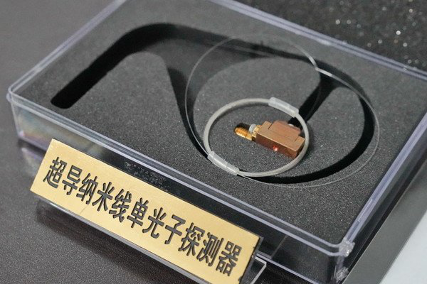
Hu Song said that the lithography machine has a maximum linewidth resolution of 22 nm in a single exposure at a wavelength of 365 nm, which is equivalent to 1/17 wavelength. In principle, the project breaks through the resolution diffraction limit and establishes a new high-resolution, large-area nanolithography equipment research and development route. It has completely independent intellectual property rights and is a revolution in metamaterials/supersurfaces, third-generation optical devices, and generalized chips. The leap-forward development of the sex field provides manufacturing tools. He specializes in processing a range of nano-functional devices, including large-diameter thin film mirrors, superconducting nanowire single photon detectors, Cherenkov radiation devices, biochemical sensor chips and ultra-surface imaging devices.

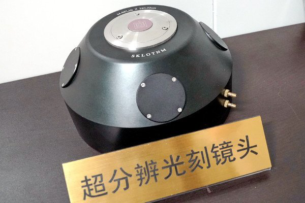
According to the report, the Institute of Optoelectronic Technology of the Chinese Academy of Sciences has mastered core patents such as super-resolution lithography lens, precision gap detection, nano-level positioning precision workpiece table, high aspect ratio etching and multiple graphic matching lithography processes. , leading the world in the field of super-resolution imaging lithography.
ASML equipment still dominates, and domestic efforts still need to work hard.
Prior to this, Shanghai Microelectronics, which was established in 2002, has taken the lead in developing a 90nm process lithography machine. Now the 22nm lithography machine developed by the Institute of Optoelectronic Technology of the Chinese Academy of Sciences has passed the acceptance test, which can be said to achieve leapfrog progress. It is understood that the related devices for the manufacture of such super-resolution lithography equipment have been studied in many research institutes and universities such as the Eighth Research Institute of China Aerospace Science and Technology Corporation, the University of Electronic Science and Technology, the West China Hospital of Sichuan University, and the Microsystems Institute of the Chinese Academy of Sciences. Applied in the task.

Although Chinese research institutes have developed new lithography machines, lithography machines developed by ASML in the Netherlands are still the first choice for Chinese customers. At the end of May this year, according to Dutch media reports, the Chinese chip giant “Yangtze Storage” shipped a $72 million lithography machine ordered from ASML to Wuhan, Hubei.
Another Japanese media reported that China's other chip maker SMIC also ordered a $120 million lithography machine from ASML, which is expected to be delivered in 2019.
Following ZTE and Fujian Jinhua, it is reported that the United States is considering sanctioning China's monitoring equipment giant Hikvision and cutting off chip supply. This will prompt China to accelerate the pace of applying domestic equipment.

