Chinese semiconductor thread II

tokenanalyst

Lieutenant General
Registered Member
10mJ/cm2 will be a golden spot for mass EUV patterning vs the current 30 mJ/cm2

Synergistic Tripartite Molecular Design of Halogen-Engineered Organotin Clusters Enabling 10 mJ cm−2 EUV Lithography​

ABSTRACT​

Organotin clusters are promising candidates for extreme ultraviolet (EUV) lithography but often suffer from insufficient sensitivity. To address this challenge, we report the first systematic library of halogen-engineered isostructural dinuclear organotin clusters (Sn2-4X, X = F, Cl, Br, I), designed to enhance EUV absorption via halogen incorporation. Our strategy features a synergistic tripartite molecular design integrating: (1) radiation-labile Sn─C bonds for efficient ionization and cleavage; (2) halogenated aromatic ligands to boost absorption cross-sections and etch resistance; and (3) triethanolamine (TEA) ligands to facilitate intermolecular cross-linking via hydrogen atom transfer (HAT). This rational engineering significantly amplifies lithographic performance. Notably, Sn2-4F achieves a record sensitivity of 10 mJ cm−2 alongside ultrahigh resolution (10 nm), establishing a new benchmark for metal–organic clusters (MOCs). Mechanistically, we reveal a fundamental dichotomy where inner-shell ionization of heavy atoms governs EUV sensitivity, whereas “kinetic overkill” dominates electron beam lithography (EBL). Furthermore, a halogen-dependent dissociative electron attachment (DEA) pathway is elucidated, which reinforces the lithographic network through Sn─X coordination. This work bridges the gap between molecular design, radiation physics, and chemistry, offering a robust roadmap for next-generation high-sensitivity EUV photoresists.
Please, Log in or Register to view URLs content!
 

tokenanalyst

Lieutenant General
Registered Member
China domestic equipment components is growing pretty fast.​

Fuchuang Precision expects its net profit to increase by up to 11 times in the first half of the year, with continued strong demand for semiconductor equipment components.​

Fuchuang Precision released its 2026 semi-annual performance forecast. The company expects to achieve a net profit attributable to owners of the parent company of RMB120 million to RMB150 million in the first half of the year, an increase of 877.49% to 1121.86% compared with the same period last year. The net profit growth rate is more than 11 times, which is extremely impressive.

In terms of revenue, the company expects to achieve operating revenue of RMB 2.1 billion to RMB 2.5 billion in the first half of the year, an increase of RMB 376 million to RMB 776 million compared with the same period last year, representing a year-on-year growth of 21.83% to 45.03%. Even calculated based on the lower limit of revenue growth, the net profit growth rate still far exceeds the revenue growth rate, reflecting a significant improvement in the company's profitability.

In its announcement, Fuchuang Precision stated that the significant increase in revenue was due to the continued improvement in the global semiconductor industry, leading to rapid order growth and a sustained expansion of revenue. Simultaneously, the company's economies of scale gradually materialized, resulting in improved gross profit margin and a marked improvement in profitability. Furthermore, the relatively low net profit base in the same period last year (approximately RMB 12.2764 million) also provided room for high growth this year.

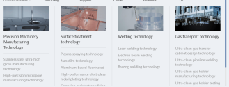
According to available information, Fuchuang Precision is a leading enterprise in the field of precision semiconductor equipment components in China. Its products cover process components, structural components, and module products, and are widely used in core semiconductor manufacturing equipment such as etching, thin film deposition, and ion implantation. The company holds an important position in the global semiconductor equipment component supply chain, and its customers include major domestic and international semiconductor equipment manufacturers.

1784567547388.png


Industry analysts point out that the global semiconductor industry chain is currently in an expansion cycle, and equipment and components, as a key upstream link in the industry chain, directly benefit from the capital expenditure expansion of downstream wafer fabs and packaging and testing plants. The exceptionally high net profit growth of Fuchuang Precision in the first half of the year reflects both the accelerated progress of domestic substitution of semiconductor equipment and components and confirms the trend of the industry's high prosperity continuing to spread upstream in the industry chain.


Please, Log in or Register to view URLs content!
 

tokenanalyst

Lieutenant General
Registered Member

Yunzhong Technology's high-performance MLCC production project, with a total investment of 1.5 billion yuan, has been signed and settled in Chizhou.​


Recently, the Management Committee of Wanjiang Jiangnan Emerging Industry Concentration Zone and Chizhou Yunzhong Electronic Technology Co., Ltd. reached an agreement, and a high-performance multilayer ceramic chip capacitor production project with a total investment of 1.5 billion yuan was successfully settled in the zone.

The project plans to construct an intelligent production line for multilayer ceramic chip capacitors in two phases, with high-performance multilayer ceramic chip capacitors as the main product. The first phase involves an investment of 750 million yuan, with construction scheduled to begin before September this year and production expected to commence by the end of the year. The second phase will be constructed separately based on the project's operational progress.

Multilayer ceramic chip capacitors are key basic components in the electronics industry, widely used in consumer electronics, automotive electronics, communications and industrial control, etc. Currently, there is broad room for domestic substitution and outstanding development potential.

On June 25, Yunzhong Technology announced that its subsidiary, Chizhou Yunzhong, plans to invest 1.5 billion yuan in a high-performance MLCC production project in Chizhou, Anhui Province. The project will be implemented in two phases, each with an investment of 750 million yuan. The implementing entity will be a newly established subsidiary, Chizhou Yunchi Electronics. The first phase of 750 million yuan will be contributed by Chizhou Yunzhong (450 million yuan) and Chizhou Jiangnan Emerging Industry Fund (300 million yuan). After the capital increase, Chizhou Yunzhong will hold 60% of the shares, and the industry fund will hold 40%. The second phase will depend on the operation of the first phase, with the company and local state-owned assets contributing another 450 million yuan and 300 million yuan respectively. Regarding the funding schedule, the industry fund's 300 million yuan contribution must be paid in by the end of October 2026, and the company's 450 million yuan contribution must be completed no later than September 2028.​

Please, Log in or Register to view URLs content!
 

siegecrossbow

Field Marshall
Staff member
Super Moderator
SemiAnalysis teardown and analyze KIRIN 9030


Technical, interesting video

Not all new, they suggest SMIC N+3 about similar to TSMC N6, but interesting to see


....a bit of cope at the end..but it's ok, they have a family to feed...
Article version for people who don’t want to sit through a video.

Please, Log in or Register to view URLs content!
 

tokenanalyst

Lieutenant General
Registered Member

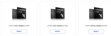
XingSi Semiconductor completes a new round of strategic industrial financing to accelerate independent innovation of 6G low-orbit satellite communication baseband chips.​


StarSemi Semiconductor has successfully completed a new round of strategic financing to accelerate its independent research and development in 6G low-orbit satellite communication baseband chips. The investment round attracted a mix of significant new investors, including state-owned entities like Xinhuan Investment (Shanghai) and Zhuzi Fang Venture Capital (Fuzhou), alongside major corporate players such as Manbang Group and Tongding Group. Existing shareholders, including General Atlantic and Langrun Lifang, have also increased their stakes to demonstrate long-term confidence in the company's mission to deepen innovation within China's low-orbit satellite internet sector.

1784645726711.png

This funding comes at a critical time as Chinese national policy continues to prioritize the development of the satellite internet industry. With the integration of satellite networks into the country's broader infrastructure plans alongside ground communication and computing grids, StarSemi's technology is positioned as a cornerstone for achieving the nation's 2030 and 2035 goals for integrated air-space-ground-sea systems. As a leading hard-tech firm, StarSemi stands out globally for its ability to fully independently design 5G/6G baseband chips from scratch. The company has already begun commercializing these technologies through solutions that enable direct satellite connectivity for smartphones and vehicles, proving the viability of domestic alternatives in this specialized market.

Looking ahead, StarSemi intends to leverage this capital not only to refine its core chip technologies but also to build a robust industrial ecosystem by collaborating with supply chain partners. The company plans to expand its portfolio of domestic satellite terminal products and push for deeper integration between satellite communications and emerging 5G-A networks. Furthermore, StarSemi aims to actively participate in the pre-research and standard-setting phases for China's 6G protocols, ensuring that the nation maintains a strong "indigenous" foundation in the global race toward high-quality, systematized space-to-earth network infrastructure.


Please, Log in or Register to view URLs content!
 

tokenanalyst

Lieutenant General
Registered Member
Article version for people who don’t want to sit through a video.

Please, Log in or Register to view URLs content!
I think Intel is having trouble getting smaller metal pitches due EUV stochastics, so is either accept these pitches or get into EUV multi-patterning which is unacceptable for Intel after paying 350 million for each of their High-NA EUV machines. My guess is one of the reasons why TSMC want to stick to Low-NA EUV machines, TSMC is the master of multi-patterning. I know I know is controversial to say that EUV is not a walk in the park.
 

tokenanalyst

Lieutenant General
Registered Member

With a total investment of 5 billion yuan, Yuanxin Microelectronics' Changsha Wangcheng Semiconductor Materials Base broke ground.​

the Yuanxin Kewei high-end display and semiconductor key material R&D and production base project officially broke ground in Changsha Wangcheng Economic Development Zone.

Yuanxin Microelectronics (Hunan) Co., Ltd. was established in December 2025. It was formed by a world-class technical team and has a deep technical foundation and industrialization experience.

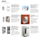
The project has a total planned investment of 5 billion yuan, with an initial investment of 1.5 billion yuan, and is located in the western extension area of the Intelligent Terminal Industrial Park in Wushan Street, Wangcheng Economic Development Zone. The factory area is planned to have a 9,218㎡ Class 10 cleanroom, equipped with a complete set of supporting facilities for semiconductor production lines, including an anti-vibration platform, ultrapure water supply, special gas transportation, waste treatment, high and low voltage power distribution, and dust-free automatic control. It aims to create an integrated industrial platform that combines technology research and development, pilot production, and large-scale mass production, with hardware standards benchmarked against leading domestic material production bases.

1784650957719.png1784650998301.png
1784651148776.png

From an industrial benefit perspective, once the project is fully completed and put into operation, it is expected to generate an annual output value of over 5 billion yuan.

Please, Log in or Register to view URLs content!
 
Last edited:

tokenanalyst

Lieutenant General
Registered Member

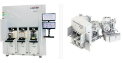
Leuven Instruments' IPO application on the Science and Technology Innovation Board has been accepted: a chemistry PhD founded a leading domestic ion beam manufacturer, and the company is backed by the National Integrated Circuit Industry Investment Fund (Big Fund) for high-growth potential across multiple categories of front-end equipment.​


The Science and Technology Innovation Board (STAR Market) has officially accepted the Initial Public Offering application from Leuven Instruments, marking a significant milestone for China's domestic semiconductor equipment sector. Founded by Xu Kaidong, a chemistry PhD with deep expertise in ion beam technology, the company is headquartered in Xuzhou, Jiangsu Province. Leuven Instruments distinguishes itself as one of the few domestic leaders capable of independently developing and mass-producing core front-end equipment across multiple categories. Backed strategically by the National Integrated Circuit Industry Investment Fund (Big Fund III), the company plans to raise 2.5 billion yuan during its IPO to accelerate the upgrade of high-end facilities and expand production capacity. This acceptance highlights Leuven's status as a "dark horse" in northern Jiangsu, possessing the rare ability to break long-standing monopolies held by overseas oligopolies in critical fields such as ion beam processing, etching, and thin film deposition.

1784655233867.png

Leuven Instruments has rapidly evolved from a specialized startup into a national-level "small giant" enterprise with over 10 years of experience in semiconductor front-end precision equipment. The company's unique value proposition lies in its ability to operate across three core technological tracks simultaneously: ion beam, ICP etching, and CVD deposition. While many domestic competitors are confined to single-product niches, Leuven Instruments has successfully penetrated the high-barrier markets of advanced logic chips, high-reliability memory, and third-generation power semiconductors. In 2025, the company entered a period of explosive commercial growth, achieving a revenue compound annual growth rate (CAGR) exceeding 80% from 2023 to 2025, with a single-year surge in 2025 that surpassed 160%. Currently, its ion beam equipment commands a dominant market share of 28.4%, and the simultaneous rollout of etching and deposition solutions allows it to provide complete process solutions to wafer fabs, creating synergistic growth opportunities far beyond those available to single-category manufacturers.​

Please, Log in or Register to view URLs content!
 
Top