Chinese semiconductor thread II

tokenanalyst

Lieutenant General
Registered Member

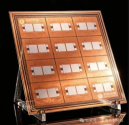
China's first glass-based CoPoS AI computing chip was officially released.​


On July 18, at the World Artificial Intelligence Conference and High-Level Meeting on Global Governance of Artificial Intelligence (WAIC 2026), Shanghai Xianfeng Technology and Suiyuan Technology , aiming to create a collaborative ecosystem of "high-performance computing chips + advanced board-level packaging", officially launched the next-generation advanced packaging solution for AI computing chips. They jointly released the first domestic and internationally leading CoPoS (Chip-on-Panel-on-Substrate) advanced board-level packaging sample for high-performance AI computing chips , filling the gap in the field of high-end computing power packaging for domestic glass-based panels. This marks a key and significant breakthrough in the research and development and industrialization of domestically produced advanced board-level packaging technology in China.

The sample released this time is a solution that combines the self-developed high-end AI computing chip of Suiyuan with the domestically produced CoPoS advanced packaging core technology for the first time. The product relies on the advanced panel-level packaging capabilities of Shanghai Xianfeng Technology, and demonstrates the iterative application of glass materials in packaging substrates, temporary carriers and other links . The product has technical advantages such as adjustable thermal expansion coefficient, extremely low high-frequency signal loss, excellent flatness and ultra-large panel molding.

Compared to traditional packaging solutions, this glass-based CoPoS packaged chip has multiple core technological advantages, including a flexibly adjustable coefficient of thermal expansion, extremely low high-frequency signal loss, excellent board flatness, and ultra-large panel forming capability. It can fully adapt to the high computing power, high frequency, and high stability operation requirements of high-end AI high-computing power chips.

1784560256504.png

Please, Log in or Register to view URLs content!
 

tokenanalyst

Lieutenant General
Registered Member

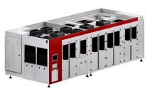
Jiejia Weichuang TGV Single-Wipe Cleaning Equipment Receives Mass Production Orders​


Recently, Jiejia Weichuang achieved another major breakthrough, with its self-developed TGV single-wafer cleaning equipment successfully securing mass production orders from leading domestic TGV companies. This marks the first time that mature semiconductor single-wafer cleaning technology has been applied to the ultra-thin glass substrate market, filling a gap in the field of key equipment for precision cleaning of domestically produced TGV products and accelerating the localization of advanced packaging equipment.

This equipment employs a single-piece cleaning architecture combined with functional water technology, enabling simultaneous cleaning of the substrate surface and edges. It deeply removes particles and organic matter from blind holes and through-holes, achieving a removal rate of over 99% for particles larger than 1μm. Simultaneously, the equipment features a Bernoulli non-contact suction cup, effectively reducing substrate fragmentation to below 10ppm, and is compatible with 80μm ultra-thin glass processing. The loading and unloading areas utilize Class 100 cleanroom management to prevent secondary contamination of the substrate.

This order signifies the successful extension of the company's wet processing equipment technology from wafers and PCBs to TGV glass substrates, creating a brand-new domestic solution for ultra-thin substrate cleaning. This not only demonstrates the core R&D capabilities of domestic semiconductor equipment companies but also provides crucial support for the independent control of the 2.5D/3D advanced packaging industry chain.​

1784560386021.png

Please, Log in or Register to view URLs content!
 

tokenanalyst

Lieutenant General
Registered Member

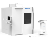
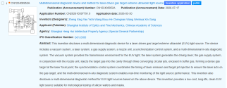
Domestically produced SiC laser lift-off equipment achieves a new breakthrough with 40% reduction in losses and compatibility with 12-inch wafers.​


Inspur Group’s subsidiary, CoreOptics, has achieved a significant breakthrough in domestic semiconductor manufacturing with the launch of a new generation of fully automated silicon carbide (SiC) laser lift-off equipment. This innovation addresses critical bottlenecks in the industry, where traditional mechanical multi-wire cutting methods have resulted in high material loss, low efficiency, and difficulties in processing larger wafers. By replacing mechanical cutting with laser stealth dicing, the new equipment utilizes a "laser internal modification + flexible layered peeling" technique. This non-contact cold processing method forms a uniform modified layer inside the SiC crystal, allowing for clean separation that minimizes mechanical stress and damage, thereby improving wafer flatness and consistency while reducing the burden on subsequent grinding and thinning processes.

The technical performance of this new equipment marks a leading level in China, having passed the technical appraisal of the Shandong Electronics Society. It offers broad compatibility with 6-inch, 8-inch, and 12-inch SiC ingots and supports customized slicing thicknesses ranging from 100 to 1500 μm. The system boasts high precision with repeatability within ±1 μm and impressive speed, processing 8-inch wafers in under 20 minutes and 12-inch wafers in under 40 minutes. Most notably, it reduces single-wafer material loss to within 80 μm, representing a approximately 40% reduction compared to traditional methods. Additionally, the process eliminates the need for consumables and chemical reagents, further driving down manufacturing costs and enhancing environmental sustainability.

1784560503979.png

Beyond its core processing capabilities, the equipment is designed for integration into modern smart factories, featuring an autonomous light source system, precision optical path control algorithms, and a closed-loop control system. It supports full automation from feeding to unloading and can seamlessly connect with MES systems, AGV logistics, and digital production lines. As the industry shifts toward 8-inch and larger SiC substrates for applications in new energy vehicles, AI computing centers, 5G communications, and power grids, this domestically produced laser lift-off solution provides a crucial pathway for capacity expansion. It promises to significantly lower costs and increase efficiency, offering high-quality large-size substrate processing solutions that support the rapid growth of these high-demand sectors.​

Please, Log in or Register to view URLs content!
 

tokenanalyst

Lieutenant General
Registered Member

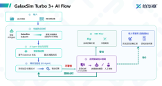
Chipone Technology (Xinhuazhang) Launches Agentic EDA 2.0 Platform at CCF Chip 2026


At the 3rd CCF Chip Conference (July 18–20, 2026), Chipone Technology unveiled its Agentic EDA base, marking a major step in its "EDA 2.0" strategy centered on an "evidence closed loop" for trusted, verifiable AI-driven chip design. The company launched the following products:
XEPIC Intelligent System (X-IS):A dual-intelligent system comprising:
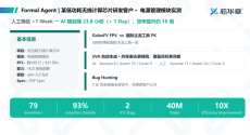
  • X-IVS (Intelligent Verification System): Integrates Simulation, Debug, and Formal Agents to automate verification. Case studies show it can detect defects and generate assertions in hours rather than days, achieving 100% coverage in complex modules.​
  • X-IDS (Intelligent Design System): Lowers hardware design barriers by using large language models to automatically repair non-synthesizable C syntax and optimize PPA (Power, Performance, Area). It links with X-IVS to ensure functional correctness during optimization. Validated with ~96% success rate in automatic correction.​
1784560945794.png
GalaxSim Turbo 3.0 Plus: A high-speed simulation solution that uses formal verification results to optimize simulation efficiency. In one NPU project, it reduced simulation time from 3 days to 1 day (3x improvement).
1784560915091.png
The Joint Venture with Wuwen Chip Universe launched an EDA AI All-in-One Machine combining Wuwen’s Mizar inference engine with Chipone’s FusionFlex platform. This integrates domestic computing power with EDA tools for scalable, secure AI chip design. The new systems support mainstream open-source and domestic large models (including DeepSeek, Zhipu, Alibaba, etc.), ensuring flexibility and data security for clients.

This launch positions Chipone as a leader in Agentic EDA, moving beyond simple AI assistance to automated, end-to-end intelligent decision-making in chip design. It aims to enhance R&D efficiency while maintaining rigorous verification standards, supporting China’s semiconductor innovation in advanced SoCs and AI chips.

Please, Log in or Register to view URLs content!
 

tokenanalyst

Lieutenant General
Registered Member

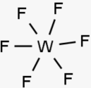
Domestically produced tungsten hexafluoride, compatible with 2nm/3nm processes and HBM!​


1784561510716.png

China Shipbuilding Special Gas Co., Ltd. (CSSC Special Gas) reported exceptional financial performance in its 2026 semi-annual results, driven by surging demand in the semiconductor sector. The company achieved a revenue of 1.904 billion yuan and a net profit attributable to the parent company of 348 million yuan in the first half of the year, representing year-on-year increases of 83.13% and 95.63%, respectively. Growth accelerated significantly in the second quarter, where revenue jumped 129.49% and net profit soared 170.51% compared to the same period last year. As a leading domestic supplier with over two decades of experience originating from the CSSC Group’s 718 Research Institute, the company has mastered core technologies across the entire production chain, ranking first in China and ninth globally in electronic specialty gas sales.

The primary catalyst for this growth is tungsten hexafluoride, an essential precursor gas for depositing tungsten films in advanced chip manufacturing, including 2nm/3nm processes and HBM memory. With no viable substitutes, this gas has become critical as global supply tightened due to production halts by major Japanese suppliers and China’s export controls on high-purity tungsten powder. Consequently, prices for 5N-grade tungsten hexafluoride surged by over 230% year-on-year. CSSC Special Gas, holding the world’s largest production capacity of 2,000 tons/year and the unique ability to mass-produce 7N-grade ultra-high purity products, saw its tungsten hexafluoride revenue nearly triple. Its customer base now includes industry giants such as TSMC, Micron, SK Hynix, and SMIC.

Beyond tungsten hexafluoride, the company maintains a diversified and robust product portfolio. It leads the global market in nitrogen trifluoride with an annual capacity of 18,500 tons, while its trifluoromethanesulfonic acid series, particularly LiTFSI for solid-state batteries, captured approximately 70% of the global market share with revenues rising over 40%.
The company is also expanding into emerging sectors such as electronic bulk gases, high-purity metals, and integrated circuit precursors. This multi-tiered strategy covers 98 products across chips, displays, lithium batteries, and pharmaceuticals, positioning CSSC Special Gas to benefit from the accelerating development of new energy vehicles and advanced semiconductor technologies.

Despite the strong profitability, the company faced a temporary cash flow challenge, with net operating cash flow dropping to -241 million yuan due to proactive stockpiling of expensive raw materials and rising accounts receivable. However, this is viewed as a short-term issue rather than a structural weakness, given the company’s solid balance sheet featuring total assets of 7.646 billion yuan and a low debt-to-asset ratio of 21.42%. With the Chinese electronic specialty gas market projected to exceed 42 billion yuan by 2030 and domestic substitution rates still low, CSSC Special Gas is well-positioned to capitalize on historic opportunities. Ongoing capacity expansions, including increasing tungsten hexafluoride output to 3,000 tons, further solidify its growth trajectory in a sector critical to national technological self-sufficiency.​

Please, Log in or Register to view URLs content!
 

tokenanalyst

Lieutenant General
Registered Member

Shandong produces its first 6N-grade high-purity hydrogen fluoride; Shandong-based company achieves breakthrough in key semiconductor materials.​


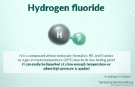
It was learned from Binhua Group that through technological breakthroughs in four areas—process, engineering, testing, and filling—the quality of its high-purity hydrogen fluoride products for semiconductors has reached the 6N grade (99.9999%), placing it at a leading level domestically and a world-class level internationally. This marks a breakthrough in my country's long-standing foreign monopoly in the field of key semiconductor materials, filling the gap in domestic high-purity hydrogen fluoride production capacity.

High-purity hydrogen fluoride gas acts like a precision "carving knife," serving as a core electronic specialty gas for critical processes in semiconductor wafer manufacturing, such as dry etching and cavity cleaning. Its purity directly determines wafer yield. 6N-grade high-purity hydrogen fluoride is essential for advanced processes at 28 nanometers and below. Previously, my country relied heavily on imports of 6N-grade high-purity hydrogen fluoride, with foreign companies monopolizing approximately 80% of the global market share.

Semiconductor-grade hydrogen fluoride requires a purity of 99.999% (5N) or higher. "The transition from 5N to 6N is not just about adding another purification step, but about establishing a completely new purification system," explained Liu Teng, General Manager of the Specialty Chemicals Division of Binhua Group. Achieving 6N purity hinges on overcoming miscible impurities in hydrogen fluoride, such as trace amounts of water, carbon dioxide, and oxygen-containing organic matter. A multi-stage distillation coupling system was designed in the rectification section. By optimizing the internal components and operating window, deep removal of carbon and oxygen impurities was achieved under a specific pressure gradient, fundamentally controlling key impurities like carbon and oxygen.
1784562339878.png

Simultaneously, the company independently developed a closed, precise sampling system and a highly sensitive analytical approach, minimizing background environmental interference during sampling to ensure that analytical data accurately reflects product quality and guaranteeing the stability and reliability of the 6N index.

Currently, the market price for 6N grade high-purity hydrogen fluoride is over 2 million yuan per ton. Binhua Group has completed the construction and commissioning of a 50-ton/year high-purity hydrogen fluoride cylinder filling line and obtained a cylinder filling license issued by the Shandong Special Equipment Inspection Institute. It has begun promoting its products to key domestic and international clients.

An evaluation meeting for the project "Key Technologies and Applications of Ultra-High Purity Electronic-Grade Hydrofluoric Acid for Advanced Semiconductor Processes," organized by the Chemical Industry and Engineering Society of China, was also held at Binhua Group. The expert panel unanimously agreed that the project's key technologies and product indicators have reached the international advanced level.

The ultra-high purity electronic-grade hydrofluoric acid project is a key R&D project (major scientific and technological innovation project) of Shandong Province, jointly completed by Binhua Group and Tianjin University. The project team successfully overcame technical bottlenecks in hydrofluoric acid purification, efficient adsorption, and key equipment for cleaning and filling, achieving continuous, large-scale, and stable production. Product indicators surpass SEMI-G5 grade, and it has been successfully adopted by 14nm advanced process semiconductor end customers, with its quality and stability recognized by leading companies in the industry.


Please, Log in or Register to view URLs content!
 
Top