Chinese semiconductor thread II

tokenanalyst

Lieutenant General
Registered Member
I took a careful look through their product lineup. It's pretty wide spread. And I wonder just how much this is about the supply chain. It's almost mind blowing you can have this many startups in such a complex industry that suddenly can produce competitive products.
That is the part that is probably disturbing a lot of foreign semi executives sleep patterns. This was supposed to be the hard part, according to US think tankers and policy advisors, that would have take decades for China to develop on its own, if ever. Now you not only see just one, but multiple companies, from the big established ones like Naura to startups, from state companies to private, from different provinces, making high end tools and variations of high end tools that was suppose, according to think tankers, difficult for China to "replicate".

Even IC metrology that was supposed to be second only to lithography, according to guy who I talked years ago, you have multiple companies basically with the entire catalog of KLA.

Now everything that these think tankers and policy advisers advised few years ago and their copes now hinge in a single Dutch company, but I think lithography is already a done deal in China, from I-Line, KrF, dry ArF, 14nm immersion this year and 7nm EUV in a few years, probably 5nm. For now the goal seem that is not to compete with ASML globally but to have patterning machines, DUV and EUV, that can meet the local demand BUT, I have to say it again, because China is not just building a single machine but an entire supply chain for lithography machines, if that supply chain is not exclusive to a single company, you could have, at least at the beginning, multiple companies entering the local lithography market, like SiCarrier and SMEE in ArF-Immersion-EUV and Naura, ACM and other startups in I-Line-KrF. Having a wild Chinese market is a big long term risk for ASML.
 

tokenanalyst

Lieutenant General
Registered Member
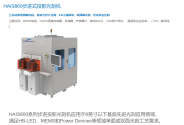
Startup making stepper projection lithography machines, imagine when they have access to advanced wafer stages, high end interferometers, high end picometer-positioning technology, high end lithography optics or even entire domestic lens assemblies, damping systems, lithography software, metrology and high end light sources like high power high repetition stable excimer lasers. Of course they will not get ASML level but they could launch pretty powerful lithography systems.

Jiangsu HiSilicon Semiconductor Technology Co., Ltd. is a professional manufacturer and supplier of stepper projection lithography machines and fully automated lithography machines (Mask Aligners) . HiSilicon's mask alignment can accommodate 300 mm products and is compatible with wafers and substrates of different shapes and thicknesses. These products are used in various fields such as MEMS, integrated circuits, hybrid modules, compound semiconductors, optoelectronic modules, 3D packaging, optical devices, power devices, and micro-nano processing.
We have established partnerships with many internationally renowned semiconductor manufacturers and research institutes. We have a professional team with extensive experience in semiconductor equipment manufacturing and lithography. HiSilicon is committed to providing customers with excellent technical solutions, continuously optimizing its business structure and improving service quality, and consistently providing high-quality services to our customers.
In June 2023, Jiangsu HiSilicon Semiconductor Technology Co., Ltd. successfully launched a stepper lithography machine and put it into the market, while simultaneously developing a 350nm resolution stepper lithography machine.
In 2024, 350nm and 500nm resolution stepper lithography machines will be officially launched.​

1762474390536.png

Please, Log in or Register to view URLs content!
 

tphuang

General
Staff member
Super Moderator
VIP Professional
Registered Member
That is the part that is probably disturbing a lot of foreign semi executives sleep patterns. This was supposed to be the hard part, according to US think tankers and policy advisors, that would have take decades for China to develop on its own, if ever. Now you not only see just one, but multiple companies, from the big established ones like Naura to startups, from state companies to private, from different provinces, making high end tools and variations of high end tools that was suppose, according to think tankers, difficult for China to "replicate".

Even IC metrology that was supposed to be second only to lithography, according to guy who I talked years ago, you have multiple companies basically with the entire catalog of KLA.

Now everything that these think tankers and policy advisers advised few years ago and their copes now hinge in a single Dutch company, but I think lithography is already a done deal in China, from I-Line, KrF, dry ArF, 14nm immersion this year and 7nm EUV in a few years, probably 5nm. For now the goal seem that is not to compete with ASML globally but to have patterning machines, DUV and EUV, that can meet the local demand BUT, I have to say it again, because China is not just building a single machine but an entire supply chain for lithography machines, if that supply chain is not exclusive to a single company, you could have, at least at the beginning, multiple companies entering the local lithography market, like SiCarrier and SMEE in ArF-Immersion-EUV and Naura, ACM and other startups in I-Line-KrF. Having a wild Chinese market is a big long term risk for ASML.
I really don't think the think tankers understand enough to look beyond what % of Lam and ASML sales still come from China region. In their mind, that means the export restrictions aren't restrictive enough.

IC metrology imo really got better in the past year as the oscilloscope and laser sensor techs got good. That's something that if you don't follow the Chinese supply chain, you just won't notice.

But it just never really seemed to me that obvious why SiGe EPI would be so difficult to do compared to other stuff, so I'm not surprised now to see so many Chinese products for it.
 

huemens

Junior Member
Registered Member

Dutch Ready to Drop Nexperia Control If Chip Supply Resumes​

Please, Log in or Register to view URLs content!
The Dutch government is ready to shelve the ministerial order that gave it the power to block or change key corporate decisions at Nexperia, if China allows exports of its critical chips again, according to people familiar with the matter.
If the shipment of supplies resumes and is verified in the coming days, the Dutch are willing to revoke its powers as soon as next week, said the people, who spoke on the condition of anonymity. Financial issues between Nexperia and its Chinese operations would also need to be resolved.
Given the constructive nature of our talks with the Chinese authorities, the Netherlands trusts that the supply of chips from China to Europe and the rest of the world will reach Nexperia’s customers over the coming days,” Dutch Economic Affairs Minister Vincent Karremans said in the statement.
A spokesperson from the economic affairs ministry declined to comment further on the situation
 

tphuang

General
Staff member
Super Moderator
VIP Professional
Registered Member

深圳平湖实验室 has unveiled GaN MPW (Multi Project Wafer) service that allows each 8-inch GaN wafer to test multiple designs over 25mm2 units/"shots". Paired with its GaN PDK to design, fab & cut/test dies so they can be taped out & validated. 650V MPW becomes available in 2025Q4 & 100V MPW in 2026Q1
 

tphuang

General
Staff member
Super Moderator
VIP Professional
Registered Member
Please, Log in or Register to view URLs content!

Garen Semi is present a new gallium oxide product (011) crystal substrate which will allow customers to dope & grow epitaxy stably. It's unclear to me based on this text on whether this is just for customers to buy and test their stuff like growing epitaxy layer and create chips or something else.
 

tokenanalyst

Lieutenant General
Registered Member

China’s Chip Equipment Industry Rides 2025 IPO Wave to Boost Localization​


Alongside acquisitions and support from national funds, China’s chip equipment sector has also welcomed a wave of new IPOs this year. In the testing equipment segment, Sidea Semiconductor Equipment was successfully listed on the Shenzhen Stock Exchange on March 24. The company focuses on developing testing tools such as probe stations and sorters, as TrendForce notes.

In the more technically demanding lithography segment, supporting and auxiliary equipment makers are also moving into the capital market. As highlighted by TrendForce, Zhongdao Optoelectronic Equipment’s IPO application has been accepted; the company primarily focuses on the R&D of semiconductor lithography equipment.

In addition, Chengdu LasTop Tech, which specializes in laser thermal processing equipment, had its STAR Market IPO application accepted in September. Laser thermal processing tools play a crucial role in key processes such as annealing. As TrendForce indicates, the industrialization of these supporting tools strengthens the overall localization of China’s lithography equipment supply chain.

Meanwhile, in the area of core components, KYKY Technology’s Beijing Stock Exchange IPO application was accepted in June. The company focuses on dry vacuum pumps and vacuum science instruments. According to TrendForce, as the “heart” of front-end high-vacuum process equipment—such as etching, PVD, and CVD tools—domestic breakthroughs in dry vacuum pumps are essential for advancing China’s semiconductor manufacturing capabilities.

Please, Log in or Register to view URLs content!
 

tokenanalyst

Lieutenant General
Registered Member

Lattice design of a storage-ring-based light source for generating high-power fully coherent EUV radiation​

Abstract​

We present the physical design and systematic optimization of a high-performance storage ring tailored for the generation of high-power coherent radiation, with particular emphasis on the extreme ultraviolet (EUV) regime. The proposed ring adopts a Double Bend Achromat (DBA) lattice configuration and integrates 12 superconducting wigglers to significantly enhance radiation damping and minimize the natural emittance. And a bypass line is adopted to generate high power coherent radiation. Comprehensive linear and nonlinear beam dynamics analyses have been conducted to ensure beam stability and robustness across the operational parameter space. The optimized design achieves a natural emittance of approximately 0.8 nm and a longitudinal damping time of around 1.4 ms, enabling the efficient buildup of coherent radiation. Three-dimensional numerical simulations, incorporating the previously proposed angular dispersion-induced microbunching (ADM) mechanism, further confirm the system’s capability to generate high-power EUV coherent radiation, with output powers reaching the order of several hundred watts. These results underscore the strong potential of the proposed design for applications in coherent photon science and EUV lithography.

Please, Log in or Register to view URLs content!
 

tokenanalyst

Lieutenant General
Registered Member

Hejian FPGA and Tsinghua Unigroup jointly build a domestic FPGA application simulation and verification ecosystem.​


Shanghai Hiview Industrial Software Group Co., Ltd. (“Hiview”), a leading Chinese digital EDA/IP company, and Shenzhen Unisplendour Electronics Co., Ltd. (“Unisplendour”) jointly announced today that they have officially joined forces to build a simulation and verification ecosystem for domestic FPGA applications. Based on Hiview’s independently developed next-generation full-featured high-performance simulator solution, UniVista Simulator Plus (UVS+), which has complete intellectual property rights, Unisplendour has authorized Hiview’s UVS+ to read encrypted IPs and other encrypted IPs in its FPGA development kit, Pango Design Suite (PDS). This will help the mutual customers of Unisplendour and Hiview use the UVS+ simulator for simulation and verification of FPGA application designs, empower the development capabilities of domestic FPGA application scenarios, promote the wider application of domestic FPGAs, and jointly build an application ecosystem for domestic EDA tools in domestic FPGAs.

Unisoc is a professional manufacturer of domestically produced programmable system platform chips and solutions, providing FPGA chips with independent intellectual property rights, supporting software tools, and system solutions. PDS software is a programmable tool suite independently developed by Unisoc, encompassing HDL description, bitstream generation, download, and debugging, providing an efficient and user-friendly integrated design environment for its entire series of FPGA chips. This software supports industry-standard development processes and already possesses the capability to support application development for large-scale FPGA chips. This collaboration signifies that Unisoc's FPGA customers can seamlessly use UVS+ for high-performance, high-reliability FPGA simulation applications. Furthermore, this collaboration between Unisoc and Hejian Software will enable its customers to adopt more domestically produced EDA tools in the domestic FPGA field, promoting the rapid development of the domestic EDA and FPGA industries, and will be a benchmark collaboration in the construction of the industrial ecosystem.

Hejian Technology's next-generation emulator, UVS+, creates a fully domestically developed one-stop verification process. Featuring a completely self-developed architecture and supporting the domestic server ecosystem, it boasts advanced simulation, compilation, and waveform processing performance comparable to leading international manufacturers, significantly accelerating the verification process. It comprehensively covers the digital simulation functions required for modern chip verification and various special application scenarios. The next-generation debugging platform, UVD+, integrates more advanced functions, providing full-scenario debugging capabilities. Its innovative data processing architecture improves verification and debugging efficiency and creates a brand-new visual experience, enhancing the debugging experience in multiple dimensions. Since the release of its first-generation product over three years ago, the UVS series has been refined and continuously optimized through millions of real-world customer project use cases. It has been successfully applied in over 50 key chip projects, gaining recognition from leading domestic customers and accumulating rich industry experience.

Please, Log in or Register to view URLs content!
 
Top