Chinese semiconductor thread II

tokenanalyst

Lieutenant General
Registered Member

Raytheon Technology receives investment from Yida Capital, a semiconductor high-end laser equipment company.​


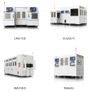
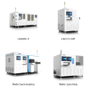
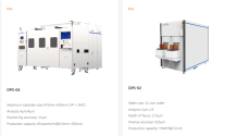
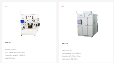
Founded in October 2021, Raytheon Technology has been focusing on the research and development and production of high-end laser equipment in the semiconductor industry. The company's main business covers key process links such as laser cutting, laser drilling, laser annealing, laser debonding, LAB laser-assisted bonding, LCB laser bonding and laser marking. It is committed to providing high-precision and high-efficiency laser processing solutions for semiconductor manufacturing . At present, the company has the capacity to produce more than 100 types of equipment annually, and has nearly 30 types of semiconductor-specific equipment on sale, which are widely used in semiconductor wafer manufacturing and advanced packaging fields to meet the needs of high-speed, high-precision and complex micro-nano processing.

Leveraging the founding team's nearly 30 years of deep industry experience and international background, Raysun Technology has developed a forward-thinking R&D strategy systems. Its products have successfully entered the supply chains of leading domestic semiconductor manufacturers and passed customer process certification, rapidly establishing itself as a rising star in the domestic high-end semiconductor laser equipment market.

According to Yida Capital, Raysun Technology founder Huang Gang stated that the company has consistently adhered to forward-thinking R&D since its founding, achieving breakthroughs in core technologies such as specialized lasers, optical control platforms, and composite motion platforms. The company's equipment, including wafer-level dicing, wafer-level slotting, wafer-level die marking, package-level uPOP drilling, and RF module TSA lamination cutting, has reached internationally leading levels in processing precision, production efficiency, and operational stability . The company's products are already gaining traction with international clients. Going forward, Raysun Technology will establish itself in the domestic market while gradually expanding its overseas presence, striving to become a leading global provider of integrated laser solutions.​

1761076233653.png1761076258467.png

Please, Log in or Register to view URLs content!
 

tokenanalyst

Lieutenant General
Registered Member

Guona Semiconductor acquires Xindao Precision to further strengthen its self-production capacity of core components for transmission equipment​

Guona Semiconductor officially announced its acquisition of Xindao Precision, furthering its commitment to unlimited possibilities. Guona Semiconductor's successful acquisition of Xindao Precision further strengthens its ability to independently produce core components for transmission equipment, enabling it to better meet customers' evolving needs and usher in the era of "full in-house production" for domestic wafer transmission equipment.

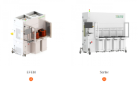
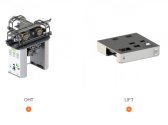
Since its founding in 2020, Guona Semiconductor has been dedicated to the research, development, and production of complete modules and key components for wafer transfer equipment, rapidly growing into a leading company in the domestic integrated circuit transfer equipment segment. The company has independently developed a range of innovative products, including front-end transfer modules (EFEMs), wafer sorters (SORTERs), wafer storage systems (STOCKERS), and automated material handling systems (AMHSs), as well as key transfer components. The company has also independently developed numerous core technologies, successfully filling gaps in this field in China.
1761076609952.png1761076632564.png
1761076659185.png1761076678047.png


The wafer front-end transport module (EFEM) is an important module of integrated circuit process and testing equipment, and is one of the essential core components of semiconductor manufacturing process equipment, testing equipment, etc. The current localization rate is still less than 50%. Precisely because of the important position of the EFEM module, Guona Semiconductor has invested a lot of R&D resources. The products currently developed and mass-produced have mastered many core technologies, have independent intellectual property rights, and can meet customers' high-end customization needs.

With such technical strength, Guona Semiconductor's products have formed industrial supporting facilities with many leading domestic semiconductor equipment companies, solving the major problem that domestic semiconductor equipment EFEM modules are heavily dependent on imports and difficult to purchase, achieving a major breakthrough in localization in this field, and effectively promoting the localization process of core components of semiconductor equipment.
Please, Log in or Register to view URLs content!
 

tokenanalyst

Lieutenant General
Registered Member

Yuanzhuo Micro-Nano Semiconductor Equipment Production Base Project Signed​


The total investment of the project is 1.5 billion yuan, and it is planned to be built in two phases. The first phase of the project is expected to be put into production in 2026. After all phases are put into production and reach full capacity, the annual output value is expected to reach 1.5 billion yuan.

According to the official WeChat account of Shangrao Economic and Technological Development Zone, a signing ceremony was held recently between Shangrao Economic and Technological Development Zone and Yuanzhuo Micronano Technology (Suzhou) Co., Ltd. (hereinafter referred to as "Yuanzhuo Micronano"), marking the official signing and implementation of the semiconductor graphics and additive manufacturing equipment production base project with a total investment of 1.5 billion yuan.

The new project is reportedly a key initiative for Yuanzhuo Micronano to expand into new markets, meet production capacity expansion, and serve customer needs. The project is planned for construction in two phases. Phase I, located in the G60 Science and Technology Innovation Corridor (Shangrao) Science and Technology Cooperation Industrial Park, is expected to begin production in 2026. Once both phases reach full capacity, the annual output value is expected to reach 1.5 billion yuan.

According to information, Yuanzhuo Micronano, as a leading company in China's high-end micro-nano processing equipment field, is a high-tech enterprise focusing on the research and development of digital laser direct writing lithography equipment and core components. Its products are mainly used in high-end equipment manufacturing fields such as chip and photovoltaic cell production, PCB board lithography and 3D printing.

1761077996971.png1761078086307.png

Please, Log in or Register to view URLs content!
 

SanWenYu

Captain
Registered Member

Raytheon Technology receives investment from Yida Capital, a semiconductor high-end laser equipment company.​


Founded in October 2021, Raytheon Technology has been focusing on the research and development and production of high-end laser equipment in the semiconductor industry. The company's main business covers key process links such as laser cutting, laser drilling, laser annealing, laser debonding, LAB laser-assisted bonding, LCB laser bonding and laser marking. It is committed to providing high-precision and high-efficiency laser processing solutions for semiconductor manufacturing . At present, the company has the capacity to produce more than 100 types of equipment annually, and has nearly 30 types of semiconductor-specific equipment on sale, which are widely used in semiconductor wafer manufacturing and advanced packaging fields to meet the needs of high-speed, high-precision and complex micro-nano processing.

Leveraging the founding team's nearly 30 years of deep industry experience and international background, Raysun Technology has developed a forward-thinking R&D strategy systems. Its products have successfully entered the supply chains of leading domestic semiconductor manufacturers and passed customer process certification, rapidly establishing itself as a rising star in the domestic high-end semiconductor laser equipment market.

According to Yida Capital, Raysun Technology founder Huang Gang stated that the company has consistently adhered to forward-thinking R&D since its founding, achieving breakthroughs in core technologies such as specialized lasers, optical control platforms, and composite motion platforms. The company's equipment, including wafer-level dicing, wafer-level slotting, wafer-level die marking, package-level uPOP drilling, and RF module TSA lamination cutting, has reached internationally leading levels in processing precision, production efficiency, and operational stability . The company's products are already gaining traction with international clients. Going forward, Raysun Technology will establish itself in the domestic market while gradually expanding its overseas presence, striving to become a leading global provider of integrated laser solutions.​

View attachment 162995View attachment 162996

Please, Log in or Register to view URLs content!
LOL on the translation of the company name. Raytheon?
 

tokenanalyst

Lieutenant General
Registered Member

On-line measurement method of ion beam machining removal function based on convolution effect correction​


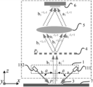
Recently, the Changchun Institute of Optics, Fine Mechanics and Physics of the Chinese Academy of Sciences published a research paper titled "Investigating a corrective online measurement method for the tool influence function in millimetre spot-sized ion beam figuring" in Light: Advanced Manufacturing . The first author of this paper is Researcher Hu Haixiang, the second author is Master's student Bian Meng, and the corresponding authors are Hu Haixiang, Tang Wa, and Ji Peng. The study proposed a high-precision online measurement method for the removal function based on convolution effect correction, which is used to calculate the small beam diameter removal function in ion beam processing online, quickly, and accurately. For removal functions with a half-height width of 0.5mm to 1mm, the calculation accuracy can be controlled at around 3%. This technology has been successfully applied to the precision shaping of large-aperture aspheric surfaces, reducing the RMS surface shape error from 1.7nm to 0.4nm in the spatial wavelength range of 15mm to 3.6mm.

The ultra-bright, highly coherent X-ray beams produced by the new generation of synchrotron radiation sources and X-ray free electron laser devices provide revolutionary tools for the exploration of the nanostructure and fundamental processes of matter. As a core optical component, the surface accuracy of the X-ray reflector directly determines the beam focusing performance and imaging quality. Among them, the surface error correction in the spatial wavelength range of 1mm to 10mm places extremely high demands on the characteristics of the processing tools. To address this problem, ion beam processing technology with extremely strong regulation flexibility of the removal function has shown great advantages. When the beam diameter of the removal function is reduced to the millimeter or even sub-millimeter level, the surface error of this part can be effectively eliminated.

In this process, accurate measurement of the small beam diameter removal function is crucial. Especially in the long-term processing of large-aperture mirrors, not only is an accurate removal function required, but its stability also needs to be monitored, evaluated, and compensated in real time, which is crucial to ensuring processing accuracy. However, experimental measurement methods cannot achieve this: the removal function data can only be obtained after processing, resulting in fluctuation compensation having to be delayed until the next round of shaping cycle. In addition, auxiliary processes such as vacuum extraction and testing further increase the time cost. Therefore, achieving high-precision online measurement of the small beam diameter removal function is the core prerequisite for improving the accuracy and efficiency of ion beam processing.

Please, Log in or Register to view URLs content!
 
Top