You are using an out of date browser. It may not display this or other websites correctly.
You should upgrade or use an alternative browser.
You should upgrade or use an alternative browser.
Chinese semiconductor thread II
- Thread starter vincent
- Start date
Yes, the development isn't limited to the EUV machine only.The one who reach the highest power and cleaness.
Also, no only lithography machines need EUV light sources but also EUV metrology and EUV mask inspection tools. China is building an entire EUV supply chain.
View attachment 162473
But it seems like EUV development is past the beginning stages, so surely the light sources that are used have already been decided? I doubt they will switch out one light source for another during the testing stages.
theoretically, but there is no evidence at this point that China will block civilian usage of rare earth components. I don't really want to speculate until there is proof for that. So, we can only say they are capable of blocking production of AI chips.China new rare earth control targeting 14nm and below. TSMC and US can say good bye to AI? China new control can shut down global tech production. Alot of materials in the fab chemical and equipments use rare earth elements.
Will depend on the modularity of the system. My guess is that all sub-systems are being develop under the same standard to be interchangeable. But I think either LDP or LPP are the current main light source of China EUV systems.Yes, the development isn't limited to the EUV machine only.
But it seems like EUV development is past the beginning stages, so surely the light sources that are used have already been decided? I doubt they will switch out one light source for another during the testing stages.
I'm pretty sure it's LPP although we don't have any sources confirming anything due to the secrecy of it all. It's just interesting to me that we are still seeing light source patents. Does anyone have any other information on which light source has progressed and/or is being integrated into early stage machines?Will depend on the modularity of the system. My guess is that all sub-systems are being develop under the same standard to be interchangeable. But I think either LDP or LPP are the current main light source of China EUV systems.
One thing I've seen frequently is that Americans on social media completely mis-interpret the wording of the government's original statement. Eg- restricting military use of RE, not some total export blockade.theoretically, but there is no evidence at this point that China will block civilian usage of rare earth components. I don't really want to speculate until there is proof for that. So, we can only say they are capable of blocking production of AI chips.
Some people just see a flashy headline on X and blow it out of proportion.
Until further notice, I think you are wise to avoid that hype and stick to the exact words from official government documents, unlike other people
Design method for wafer alignment marks with low alignment position deviation under process-induced asymmetry.
Abstract
High-precision wafer alignment is a key technology for achieving high overlay accuracy in advanced-node semiconductor manufacturing. In immersion, extreme ultraviolet (EUV), and high-NA EUV lithography, asymmetry in alignment mark structures, introduced by processes, such as chemical–mechanical polishing, is a primary cause of alignment position deviation (APD), which significantly degrades overlay accuracy. To address this issue at its root, this paper presents a systematic design methodology for segmented grating alignment marks based on multi-objective optimization. The mark geometry is parameterized and coupled with finite-difference time-domain simulations. A non-dominated sorting genetic algorithm (NSGA-II) is employed to simultaneously maximize diffraction efficiency and minimize APD under asymmetric deformation. Optimization results for two design examples confirm the effectiveness and feasibility of the proposed approach.
Maike Technology Completes RMB100 Million Series A Financing, Fully Increasing Investment in TGV Core Technology
Maike Technology, a technology transfer company funded by the University of Electronic Science and Technology of China, has completed a RMB 100 million Series A financing round. The funds will be primarily invested in research and development and production of Through-Glass Via (TGV) technology, reinforcing its leadership in advanced semiconductor packaging.
As a national high-tech enterprise with designations including "Specialized, Advanced, and Innovative" SME and lead unit in a National Key R&D Program, Maike Technology has pioneered TGV3.0 a breakthrough enabling sub-10-micron through-holes and vertical interconnects making it one of the earliest Chinese companies to develop TGV technology. The company has won prestigious awards such as the National Innovation Medal and Sichuan Provincial Technology Invention Award.
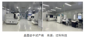
Maike has established a comprehensive production ecosystem: its subsidiary Triassic (Guangdong) operates a competitive international-grade wafer-level TGV process line in Dongguan, while Triassic (Sichuan) serves as R&D base for glass wafer 3D packaging in Chongzhou. This makes Maike the only global company capable of both wafer- and panel-level TGV production.
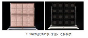
Key products include high-density large-area TGV substrates used in 2.5D computing chip packaging, now supplied stably to leading semiconductor and display firms; 3D RF/optoelectronic adapter plates supporting communications, radar, and data centers and foldable display backplanes that have passed rigorous testing by Schott AG and top domestic display companies, currently being supplied in small batches to major smartphone manufacturers.
With the Series A funding, Maike plans to: intensify TGV R&D and production to solidify technological leadership drive mass production of 2–3 core products to accelerate industrialization; integrate industry resources to build a TGV ecological innovation center attract innovative IC companies and establish the TGV Industry Alliance. The initiative aims to advance China’s self-reliance in post-Moore era semiconductor packaging, delivering a unique domestic solution for next-generation electronics.
As a national high-tech enterprise with designations including "Specialized, Advanced, and Innovative" SME and lead unit in a National Key R&D Program, Maike Technology has pioneered TGV3.0 a breakthrough enabling sub-10-micron through-holes and vertical interconnects making it one of the earliest Chinese companies to develop TGV technology. The company has won prestigious awards such as the National Innovation Medal and Sichuan Provincial Technology Invention Award.
Maike has established a comprehensive production ecosystem: its subsidiary Triassic (Guangdong) operates a competitive international-grade wafer-level TGV process line in Dongguan, while Triassic (Sichuan) serves as R&D base for glass wafer 3D packaging in Chongzhou. This makes Maike the only global company capable of both wafer- and panel-level TGV production.

Key products include high-density large-area TGV substrates used in 2.5D computing chip packaging, now supplied stably to leading semiconductor and display firms; 3D RF/optoelectronic adapter plates supporting communications, radar, and data centers and foldable display backplanes that have passed rigorous testing by Schott AG and top domestic display companies, currently being supplied in small batches to major smartphone manufacturers.

With the Series A funding, Maike plans to: intensify TGV R&D and production to solidify technological leadership drive mass production of 2–3 core products to accelerate industrialization; integrate industry resources to build a TGV ecological innovation center attract innovative IC companies and establish the TGV Industry Alliance. The initiative aims to advance China’s self-reliance in post-Moore era semiconductor packaging, delivering a unique domestic solution for next-generation electronics.
Feinan Laser's water-guided laser equipment demonstrates its strength in diamond processing
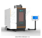
Feina Laser has independently developed water-guided laser cutting equipment. The company has launched multiple models of water-guided laser cutting equipment, including three-axis and five-axis models, equipped with multiple optional modules. The company has also achieved process matching with leading domestic customers across multiple industries, completing cutting processes for samples from various industries, primarily involving silicon carbide, silicon carbide composites, high-temperature alloys, diamond, carbon fiber composites, GaAs, magnetic materials, and other materials. The company has also secured multiple orders from the diamond industry, among others.
Three-axis and five-axis water-guided laser cutting equipment, incorporating cutting-edge technology, are revolutionizing materials processing. Their core principle is to precisely couple a high-power laser beam into an extremely fine (30-80 μm) water jet. The water jet acts as a "guide," not only guiding the laser beam but also rapidly cooling the workpiece during cutting, ensuring a clean cut surface with no heat-affected zone. Three-axis systems offer three degrees of freedom (X, Y, and Z), enabling high precision and minimal kerf width. Five-axis systems utilize a highly stable cradle-like configuration with X, Y, and Z linear axes and two rotary axes, enabling multi-dimensional cutting. They can also be tilted for cutting and punching, enabling multi-dimensional cutting, bringing a new level of efficiency and quality to production.
Water-guided laser cutting of diamonds uses non-contact cold processing, rapidly dissipating heat through water flow. The heat-affected zone is almost negligible, avoiding stress damage to the diamond and preserving its excellent performance . The cutting accuracy reaches the micron level, enabling the processing of complex and fine structures with a high surface finish and no secondary treatment. At the same time, the water flow flushes away debris, making the processing environmentally friendly and efficient, significantly reducing material loss , and providing a high-quality solution for high-end diamond applications.
With its independently developed water-guided laser cutting equipment, PhiNano Laser has accumulated numerous successful cases in the diamond cutting field. In the semiconductor industry, it has cut diamond heat sinks for many well-known chip manufacturers , helping them dissipate heat efficiently and improve operational stability. In the jewelry processing industry, it has helped numerous high-end jewelry brands achieve precise cutting of complex diamond shapes , adding a touch of flair and uniqueness to their designs. At scientific research institutions, it has assisted in cutting-edge research on diamond materials, providing strong processing support for the development of new functional materials. These extensive application cases fully demonstrate the strength and wide applicability of PhiNano Laser's water-guided laser equipment in the diamond cutting field.
Three-axis and five-axis water-guided laser cutting equipment, incorporating cutting-edge technology, are revolutionizing materials processing. Their core principle is to precisely couple a high-power laser beam into an extremely fine (30-80 μm) water jet. The water jet acts as a "guide," not only guiding the laser beam but also rapidly cooling the workpiece during cutting, ensuring a clean cut surface with no heat-affected zone. Three-axis systems offer three degrees of freedom (X, Y, and Z), enabling high precision and minimal kerf width. Five-axis systems utilize a highly stable cradle-like configuration with X, Y, and Z linear axes and two rotary axes, enabling multi-dimensional cutting. They can also be tilted for cutting and punching, enabling multi-dimensional cutting, bringing a new level of efficiency and quality to production.
Water-guided laser cutting of diamonds uses non-contact cold processing, rapidly dissipating heat through water flow. The heat-affected zone is almost negligible, avoiding stress damage to the diamond and preserving its excellent performance . The cutting accuracy reaches the micron level, enabling the processing of complex and fine structures with a high surface finish and no secondary treatment. At the same time, the water flow flushes away debris, making the processing environmentally friendly and efficient, significantly reducing material loss , and providing a high-quality solution for high-end diamond applications.

With its independently developed water-guided laser cutting equipment, PhiNano Laser has accumulated numerous successful cases in the diamond cutting field. In the semiconductor industry, it has cut diamond heat sinks for many well-known chip manufacturers , helping them dissipate heat efficiently and improve operational stability. In the jewelry processing industry, it has helped numerous high-end jewelry brands achieve precise cutting of complex diamond shapes , adding a touch of flair and uniqueness to their designs. At scientific research institutions, it has assisted in cutting-edge research on diamond materials, providing strong processing support for the development of new functional materials. These extensive application cases fully demonstrate the strength and wide applicability of PhiNano Laser's water-guided laser equipment in the diamond cutting field.
theoretically, but there is no evidence at this point that China will block civilian usage of rare earth components. I don't really want to speculate until there is proof for that. So, we can only say they are capable of blocking production of AI chips.
it's 14nm or below for semiconductor production requires permit on a case by case,
Even if it contains 0.1% of Chinese rare earth or tech. I heard this was initiated by Pakistan using chinese tech and equipments to process and export rare earth to US. That and Trump 's new tariffs on Chinese ships prompts China strong new response.
If trumps slap additional 100% tariffs on all Chinese goods which becomes 155%, I think China then would bring down TSMC and that would bring down entire west tech sector.
So depending how Trump reacts the new rule.
