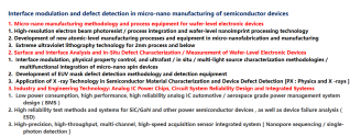
The grapevine can’t seem to decide if the Huawei instrument is LDP or LPP.This seems rather ambitious. I find the claims here to be a little beyond belief although I can believe Sicarrier EUV is testing out at SMIC fab somewhere
View attachment 161912
You are using an out of date browser. It may not display this or other websites correctly.
You should upgrade or use an alternative browser.
You should upgrade or use an alternative browser.
Chinese semiconductor thread II
- Thread starter vincent
- Start date
To be fair, there are multiple projects and machines at various stages so that might be causing the confusion.The grapevine can’t seem to decide if the Huawei instrument is LDP or LPP.
Most of this stuff is just rumors with no proof of credibility.
The biggest giveaway that EUV is coming was Huawei's AI chip roadmap. The chips in 2028 require advanced nodes that would need EUV in some form.
If they feel confident projecting that onto a big screen, they are probably confident about EUV situation.
Apart from that, rumours about Huawei or EUV in general can't be confirmed, but probably worth noting.
Yes but specifically I am hearing the Huawei owned project is LDP from one person and LPP from another. Unless Huawei owns more than one project (which I doubt but maybe?) This is a square contradiction. Either way someone out there knows what the actual factual details are lol. If we’re this close to initial adoption it would be nice to know what those details are.To be fair, there are multiple projects and machines at various stages so that might be causing the confusion.
Most of this stuff is just rumors with no proof of credibility.
The biggest giveaway that EUV is coming was Huawei's AI chip roadmap. The chips in 2028 require advanced nodes that would need EUV in some form.
If they feel confident projecting that onto a big screen, they are probably confident about EUV situation.
Apart from that, rumours about Huawei or EUV in general can't be confirmed, but probably worth noting.
Last edited:
Its correlate with the findings we have found here, EUV masks, photoresist and reticle fabrication and defect inspection technology. The have been testing this device for quite some time outside a lab environment. Trial production. Now 150 WPH is quite ambitious but possible with 250 Watts of LDP power.This seems rather ambitious. I find the claims here to be a little beyond belief although I can believe Sicarrier EUV is testing out at SMIC fab somewhere
View attachment 161912
EUV mirrors most likely from CIOMP.Its correlate with the findings we have found here, EUV masks, photoresist and reticle fabrication and defect inspection technology. The have been testing this device for quite some time outside a lab environment. Trial production. Now 150 WPH is quite ambitious but possible with 250 Watts of LDP power.
SIOMP too in this category.
The information in it is very inconsistent.
It says they are trailing it in SMIC Beijing 200mm fab to verify 5nm node. All SMIC Beijing fabs are 300mm and mature node. If they are verifying 5nm node, most ideal location is Shanghai.
It also claims SMEE is trying LPP route. But from everything we have seen here before, SMEE is not involved in EUV litho, perhaps other than the MET we saw earlier.
Then it says v1 throughput is 10 WPH and v2 throughput will be 150 WPH. Then in the next paragraph it says it can process 250 wafers per hour surpassing ASML's 190 (which is not accurate either).
SMIC still have 200mm fabs. Makes sense to trial the machine the machine in a 200mm wafer pilot line, for now, increasing the wafer size to 300mm would collapse the throughput. My guess 250 WPH is the final goal.The information in it very inconsistent.
It says they are trailing it in SMIC Beijing 200mm fab to verify 5nm node. All SMIC Beijing fabs are 300mm and mature node. If they are verifying 5nm node, most ideal location is Shanghai.
Yes, But all their Bejing fabs are 300mm. 200mm fabs are in other cities.SMIC still have 200mm fabs. Makes sense to trial the machine the machine in a 200mm wafer pilot line, for now, increasing the wafer size to 300mm would collapse the throughput. My guess 250 WPH is the final goal.
And this post started appearing in social media several months ago. At that time it did not have the above things I mentioned, so most likely people just made up and added things on their own as they went on passing the rumor.

